|
|
|
PDF AT45DB041-JC Data sheet ( Hoja de datos )
| Número de pieza | AT45DB041-JC | |
| Descripción | 4-Megabit 2.7-volt Only Serial DataFlash | |
| Fabricantes | ATMEL Corporation | |
| Logotipo | ||
Hay una vista previa y un enlace de descarga de AT45DB041-JC (archivo pdf) en la parte inferior de esta página. Total 18 Páginas | ||
|
No Preview Available !
Features
• Single 2.7V - 3.6V Supply
• Serial Interface Architecture
• Page Program Operation
– Single Cycle Reprogram (Erase and Program)
– 2048 Pages (264 Bytes/Page) Main Memory
• Two 264-Byte SRAM Data Buffers – Allows Receiving of Data
While Reprogramming of Non-Volatile Memory
• Internal Program and Control Timer
• Fast Page Program Time – 7 ms Typical
• 120 µs Typical Page to Buffer Transfer Time
• Low Power Dissipation
– 4 mA Active Read Current Typical
– 8 µA CMOS Standby Current Typical
• 5 MHz Max Clock Frequency
• Hardware Data Protection Feature
• Serial Peripheral Interface (SPI) Compatible – Modes 0 and 3
• CMOS and TTL Compatible Inputs and Outputs
• Commercial and Industrial Temperature Ranges
Description
The AT45DB041 is a 2.7-volt only, serial interface Flash memory suitable for in-sys-
tem reprogramming. Its 4,325,376 bits of memory are organized as 2048 pages of
264-bytes each. In addition to the main memory, the AT45DB041 also contains two
SRAM data buffers of 264-bytes each. The buffers allow receiving of data while a
page in the main memory is being reprogrammed. Unlike conventional Flash memo-
ries that are accessed randomly with multiple address lines and a parallel interface,
the DataFlash uses a serial interface to sequentially access its data. The simple serial
interface facilitates hardware layout, increases system reliability, minimizes switching
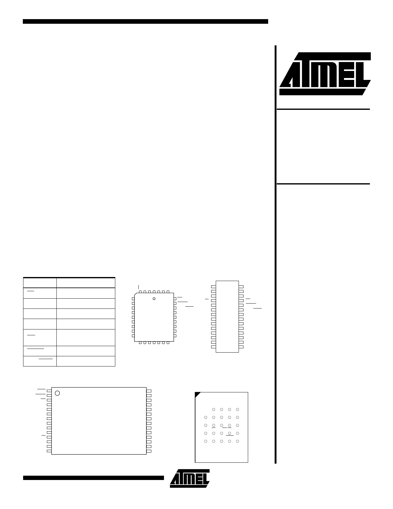
Pin Configurations
PLCC
(continued)
SOIC
Pin Name
CS
SCK
SI
SO
WP
RESET
RDY/BUSY
Function
Chip Select
Serial Clock
Serial Input
Serial Output
Hardware Page Write
Protect Pin
Chip Reset
Ready/Busy
SCK
SI
SO
NC
NC
NC
NC
NC
NC
5
6
7
8
9
10
11
12
13
29 WP
28 RESET
27 RDY/BUSY
26 NC
25 NC
24 NC
23 NC
22 NC
21 NC
GND
NC
NC
CS
SCK
SI
SO
NC
NC
NC
NC
NC
NC
NC
Note: PLCC package pins 16
and 17 are DON’T CONNECT.
1
2
3
4
5
6
7
8
9
10
11
12
13
14
28 VCC
27 NC
26 NC
25 WP
24 RESET
23 RDY/BUSY
22 NC
21 NC
20 NC
19 NC
18 NC
17 NC
16 NC
15 NC
RDY/BUSY
RESET
WP
NC
NC
VCC
GND
NC
NC
NC
CS
SCK
SI
SO
1
2
3
4
5
6
7
8
9
10
11
12
13
14
TSOP Top View
Type 1
28 NC
27 NC
26 NC
25 NC
24 NC
23 NC
22 NC
21 NC
20 NC
19 NC
18 NC
17 NC
16 NC
15 NC
CBGA Top View
Through Package
12345
A
NC NC NC NC
B
NC SCK GND VCC NC
C
NC CS RDY/BSY WP NC
D
NC SO SI RESET NC
E
NC NC NC NC NC
4-Megabit
2.7-volt Only
Serial
DataFlash®
AT45DB041
Rev. 0669D–07/98
1
1 page 
AT45DB041
RESET: A low state on the reset pin (RESET) will terminate
the operation in progress and reset the internal state
machine to an idle state. The device will remain in the reset
condition as long as a low level is present on the RESET
pin. Normal operation can resume once the RESET pin is
brought back to a high level.
The device also incorporates an internal power-on reset
circuit; therefore, there are no restrictions on the RESET
pin during power-on sequences.
READY/BUSY: This open drain output pin will be driven
low when the device is busy in an internally self-timed oper-
ation. This pin, which is normally in a high state (through an
external pull-up resistor), will be pulled low during program-
Absolute Maximum Ratings*
Temperature Under Bias ................................ -55°C to +125°C
Storage Temperature ..................................... -65°C to +150°C
All Input Voltages
(including NC Pins)
with Respect to Ground ...................................-0.6V to +6.25V
All Output Voltages
with Respect to Ground .............................-0.6V to VCC + 0.6V
ming operations, compare operations, and during page-to-
buffer transfers.
The busy status indicates that the Flash memory array and
one of the buffers cannot be accessed; read and write
operations to the other buffer can still be performed.
Power On/Reset State
When power is first applied to the device, or when recover-
ing from a reset condition, the device will default to SPI
mode 3. In addition, the SO pin will be in a high impedance
state, and a high to low transition on the CS pin will be
required to start a valid instruction. The SPI mode will be
automatically selected on every falling edge of CS by sam-
pling the inactive clock state.
*NOTICE:
Stresses beyond those listed under “Absolute
Maximum Ratings” may cause permanent dam-
age to the device. This is a stress rating only and
functional operation of the device at these or any
other conditions beyond those indicated in the
operational sections of this specification is not
implied. Exposure to absolute maximum rating
conditions for extended periods may affect device
reliability.
DC and AC Operating Range
AT45DB041
Operating Temperature (Case)
VCC Power Supply(1)
Com.
Ind.
0°C to 70°C
-40°C to 85°C
2.7V to 3.6V
Note: 1. After power is applied and VCC is at the minimum specified data sheet value, the system should wait 20 ms before an oper-
ational mode is started.
5
5 Page 
AT45DB041
Detailed Bit-Level Read Timing – Inactive Clock Polarity Low
Main Memory Page Read
CS
SCK
tSU
SI
SO
12345
60 61 62 63 64 65 66 67
COMMAND OPCODE
01010
XXXXX
HIGH-IMPEDANCE
tV
DATA OUT
D7 D6
MSB
D5
Buffer Read
CS
SCK
tSU
SI
SO
12345
36 37 38 39 40 41 42 43
COMMAND OPCODE
01010
XXXXX
HIGH-IMPEDANCE
tV
DATA OUT
D7 D6
MSB
D5
Status Register Read
CS
SCK
tSU
SI
SO
1 2 3 4 5 6 7 8 9 10 11 12
16 17
COMMAND OPCODE
01010111
HIGH-IMPEDANCE
tV
STATUS REGISTER OUTPUT
D7 D6
MSB
D5
D1 D0 D7
LSB MSB
11
11 Page | ||
| Páginas | Total 18 Páginas | |
| PDF Descargar | [ Datasheet AT45DB041-JC.PDF ] | |
Hoja de datos destacado
| Número de pieza | Descripción | Fabricantes |
| AT45DB041-JC | 4-Megabit 2.7-volt Only Serial DataFlash | ATMEL Corporation |
| AT45DB041-JI | 4-Megabit 2.7-volt Only Serial DataFlash | ATMEL Corporation |
| Número de pieza | Descripción | Fabricantes |
| SLA6805M | High Voltage 3 phase Motor Driver IC. |
Sanken |
| SDC1742 | 12- and 14-Bit Hybrid Synchro / Resolver-to-Digital Converters. |
Analog Devices |
|
DataSheet.es es una pagina web que funciona como un repositorio de manuales o hoja de datos de muchos de los productos más populares, |
| DataSheet.es | 2020 | Privacy Policy | Contacto | Buscar |