|
|
PDF AT49BV001AN Data sheet ( Hoja de datos )
| Número de pieza | AT49BV001AN | |
| Descripción | 1-megabit (128K x 8) Single 2.7-volt Battery-Voltage Flash Memory | |
| Fabricantes | ATMEL Corporation | |
| Logotipo |  |
|
Hay una vista previa y un enlace de descarga de AT49BV001AN (archivo pdf) en la parte inferior de esta página. Total 18 Páginas | ||
|
No Preview Available !
Features
• Single Supply for Read and Write: 2.7 to 3.6V
• Fast Read Access Time – 55 ns
• Internal Program Control and Timer
• Sector Architecture
– One 16K Bytes Boot Block with Programming Lockout
– Two 8K Bytes Parameter Blocks
– Two Main Memory Blocks (32K Bytes, 64K Bytes)
• Fast Erase Cycle Time – 3 Seconds
• Byte-by-Byte Programming – 30 µs/Byte Typical
• Hardware Data Protection
• DATA Polling for End of Program Detection
• Low Power Dissipation
– 15 mA Active Current
– 50 µA CMOS Standby Current
• Typical 10,000 Write Cycles
Description
The AT49BV001A(N)(T) is a 2.7-volt-only in-system reprogrammable Flash Memory.
Its 1 megabit of memory is organized as 131,072 words by 8 bits. Manufactured with
Atmel’s advanced nonvolatile CMOS technology, the device offers access times to
55 ns with power dissipation of just 54 mW over the industrial temperature range.
Pin Configurations
Pin Name
A0 - A16
CE
OE
WE
RESET
I/O0 - I/O7
NC
Function
Addresses
Chip Enable
Output Enable
Write Enable
RESET
Data Inputs/Outputs
No Connect
PLCC Top View
VSOP Top View (8 x 14 mm) or
TSOP Top View (8 x 20 mm)
Type 1
A11
A9
A8
A13
A14
NC
WE
VCC
*RESET
A16
A15
A12
A7
A6
A5
A4
1
2
3
4
5
6
7
8
9
10
11
12
13
14
15
16
32 OE
31 A10
30 CE
29 I/O7
28 I/O6
27 I/O5
26 I/O4
25 I/O3
24 GND
23 I/O2
22 I/O1
21 I/O0
20 A0
19 A1
18 A2
17 A3
1-megabit
(128K x 8)
Single 2.7-volt
Battery-Voltage™
Flash Memory
AT49BV001A
AT49BV001AN
AT49BV001AT
AT49BV001ANT
A7 5
A6 6
A5 7
A4 8
A3 9
A2 10
A1 11
A0 12
I/O0 13
29 A14
28 A13
27 A8
26 A9
25 A11
24 OE
23 A10
22 CE
21 I/O7
Note: *This pin is a NC on the AT49BV001AN(T).
Rev. 3364C–FLASH–9/03
1
1 page 
AT49BV001A(N)(T)
DATA POLLING: The AT49BV001A(N)(T) features DATA polling to indicate the end of a pro-
gram cycle. During a program cycle an attempted read of the last byte loaded will result in the
complement of the loaded data on I/O7. Once the program cycle has been completed, true
data is valid on all outputs and the next cycle may begin. DATA polling may begin at any time
during the program cycle.
TOGGLE BIT: In addition to DATA polling the AT49BV001A(N)(T) provides another method
for determining the end of a program or erase cycle. During a program or erase operation,
successive attempts to read data from the device will result in I/O6 toggling between one and
zero. Once the program cycle has completed, I/O6 will stop toggling and valid data will be
read. Examining the toggle bit may begin at any time during a program cycle.
HARDWARE DATA PROTECTION: Hardware features protect against inadvertent programs
to the AT49BV001A(N)(T) in the following ways: (a) VCC sense: if VCC is below 1.8V (typical),
the program function is inhibited. (b) Program inhibit: holding any one of OE low, CE high or
WE high inhibits program cycles. (c) Noise filter: pulses of less than 15 ns (typical) on the WE
or CE inputs will not initiate a program cycle.
3364C–FLASH–9/03
5
5 Page 
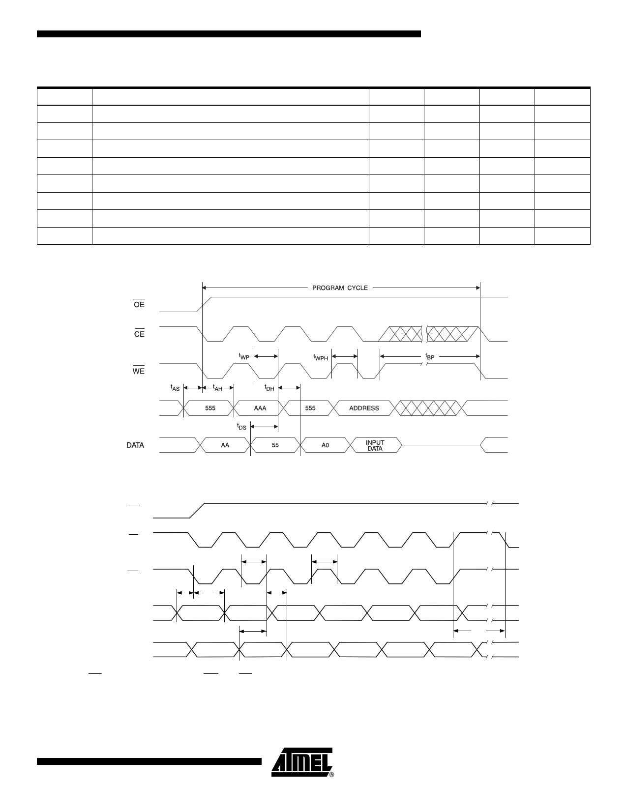
Program Cycle Characteristics
Symbol
tBP
tAS
tAH
tDS
tDH
tWP
tWPH
tEC
Parameter
Byte Programming Time
Address Set-up Time
Address Hold Time
Data Set-up Time
Data Hold Time
Write Pulse Width
Write Pulse Width High
Erase Cycle Time
Program Cycle Waveforms
AT49BV001A(N)(T)
Min Typ Max Units
30 50 µs
0 ns
40 ns
40 ns
0 ns
30 ns
30 ns
3 5 seconds
A0 - A16
Sector or Chip Erase Cycle Waveforms
OE (1)
CE
WE
tAS
tWP
tAH tDH
tWPH
A0 - A16
555 AAA
555
555
AAA
Note 2
tDS tEC
Notes:
DATA
AA 55 80 AA 55 Note 3
BYTE 0
BYTE 1
BYTE 2
BYTE 3
BYTE 4
BYTE 5
1. OE must be high only when WE and CE are both low.
2. For chip erase, the address should be 555. For sector erase, the address depends on what sector is to be erased.
(See note 4 under command definitions.)
3. For chip erase, the data should be 10H, and for sector erase, the data should be 30H.
3364C–FLASH–9/03
11
11 Page | ||
| Páginas | Total 18 Páginas | |
| PDF Descargar | [ Datasheet AT49BV001AN.PDF ] | |
Hoja de datos destacado
| Número de pieza | Descripción | Fabricantes |
| AT49BV001A | 1-megabit (128K x 8) Single 2.7-volt Battery-Voltage Flash Memory | ATMEL Corporation |
| AT49BV001A-55JI | 1-megabit (128K x 8) Single 2.7-volt Battery-Voltage Flash Memory | ATMEL Corporation |
| AT49BV001A-55TI | 1-megabit (128K x 8) Single 2.7-volt Battery-Voltage Flash Memory | ATMEL Corporation |
| AT49BV001A-55VI | 1-megabit (128K x 8) Single 2.7-volt Battery-Voltage Flash Memory | ATMEL Corporation |
| Número de pieza | Descripción | Fabricantes |
| SLA6805M | High Voltage 3 phase Motor Driver IC. |
Sanken |
| SDC1742 | 12- and 14-Bit Hybrid Synchro / Resolver-to-Digital Converters. |
Analog Devices |
|
DataSheet.es es una pagina web que funciona como un repositorio de manuales o hoja de datos de muchos de los productos más populares, |
| DataSheet.es | 2020 | Privacy Policy | Contacto | Buscar |
