|
|
PDF AT49BV8192AT-20TC Data sheet ( Hoja de datos )
| Número de pieza | AT49BV8192AT-20TC | |
| Descripción | 8-Megabit 1M x 8/ 512K x 16 CMOS Flash Memory | |
| Fabricantes | ATMEL Corporation | |
| Logotipo |  |
|
Hay una vista previa y un enlace de descarga de AT49BV8192AT-20TC (archivo pdf) en la parte inferior de esta página. Total 16 Páginas | ||
|
No Preview Available !
Features
• 2.7V to 3.6V Read/Write Operation
• Fast Read Access Time - 120 ns
• Internal Erase/Program Control
• Sector Architecture
– One 8K Words (16K bytes) Boot Block with Programming Lockout
– Two 4K Words (8K bytes) Parameter Blocks
– One 496K Words (992K bytes) Main Memory Array Block
• Fast Sector Erase Time - 10 seconds
• Byte-by-Byte or Word-By-Word Programming - 30 µs Typical
• Hardware Data Protection
• DATA Polling For End Of Program Detection
• Low-Power Dissipation
– 25 mA Active Current
– 50 µA CMOS Standby Current
• Typical 10,000 Write Cycles
Description
The AT49BV008A(T) and AT49BV8192A(T) are 3-volt, 8-megabit Flash Memories
organized as 1,048,576 words of 8 bits each or 512K words of 16 bits each. Manufac-
tured with Atmel’s advanced nonvolatile CMOS technology, the devices offer access
times to 120 ns with power dissipation of just 67 mW at 2.7V read. When deselected,
the CMOS standby current is less than 50 µA.
The device contains a user-enabled “boot block” protection feature. Two versions of
the feature are available: the AT49BV008A/8192A locates the boot block at lowest
order addresses (“bottom boot”); the AT49BV008AT/8192AT locates it at highest
order addresses (“top boot”).
To allow for simple in-system reprogrammability, the AT49BV008A(T)/8192A(T) does
not require high input voltages for programming. Reading data out of the device is
similar to reading from an EPROM; it has standard CE, OE, and WE inputs to avoid
bus contention. Reprogramming the AT49BV008A(T)/8192A(T) is performed by first
erasing a block of data and then programming on a byte-by-byte or word-by-word
basis.
(continued)
Pin Configurations
Pin Name
A0 - A18
CE
OE
WE
RESET
RDY/BUSY
VPP
I/O0 - I/O14
I/O15 (A-1)
BYTE
NC
Function
Addresses
Chip Enable
Output Enable
Write Enable
Reset
Ready/Busy Output
Optional Power Supply for Faster
Program/Erase Operations
Data Inputs/Outputs
I/O15 (Data Input/Output, Word Mode)
A-1 (LSB Address Input, Byte Mode)
Selects Byte or Word Mode
No Connect
8-Megabit
(1M x 8/
512K x 16)
CMOS Flash
Memory
AT49BV008A
AT49BV008AT
AT49BV8192A
AT49BV8192AT
Preliminary
Rev. 1049C–09/98
1
1 page 
AT49BV008A(T)/8192A(T)
For details, see Operating Modes (for hardware operation)
or Software Product Identification. The manufacturer and
device code is the same for both modes.
DATA POLLING: The AT49BV008A(T)/8192A(T) features
DATA polling to indicate the end of a program cycle. During
a program cycle an attempted read of the last byte loaded
will result in the complement of the loaded data on I/O7.
Once the program cycle has been completed, true data is
valid on all outputs and the next cycle may begin. During a
chip or sector erase operation, an attempt to read the
device will give a “0” on I/O7. Once the program or erase
cycle has completed, true data will be read from the device.
DATA polling may begin at any time during the program
cycle.
T O G G L E B I T : I n a d d i t i o n t o DATA p o l l i n g t h e
AT49BV008A(T)/8192A(T) provides another method for
determining the end of a program or erase cycle. During a
program or erase operation, successive attempts to read
data from the device will result in I/O6 toggling between
one and zero. Once the program cycle has completed, I/O6
will stop toggling and valid data will be read. Examining the
toggle bit may begin at any time during a program cycle.
READY/BUSY: For the AT49F008A(T), pin 12 is an open
drain READY/BUSY output pin which provides another
method of detecting the end of a program or erase opera-
tion. RDY/BUSY is actively pulled low during the internal
program and erase cycles and it is released at the comple-
tion of the cycle. The open drain connection allows for OR-
tying of several devices to the same RDY/BUSY line.
HARDWARE DATA PROTECTION: Hardware features
protect against inadvertent programs to the
AT49BV008A(T)/8192A(T) in the following ways: (a) VCC
sense: if VCC is below 1.8V (typical), the program function
is inhibited. (b) VCC power on delay: once VCC has reached
the VCC sense level, the device will automatically time out
10 ms (typical) before programming. (c) Program inhibit:
holding any one of OE low, CE high or WE high inhibits
program cycles. (d) Noise filter: pulses of less than 15 ns
(typical) on the WE or CE inputs will not initiate a program
cycle.
INPUT LEVELS: While operating with a 2.7V to 3.6V
power supply, the address inputs and control inputs (OE,
CE, and WE) may be driven from 0 to 5.5V without
adversely affecting the operation of the device. The I/O
lines can only be driven from 0 to VCC + 0.6V.
AT49BV008A(T) ALTERNATE PIN DEFINITION: Two
AT49BV008A(T) BGA pin definitions are shown. The stan-
dard pin definition allows use of the JEDEC standard pro-
gramming algorithm. If the alternate pin definition is used,
the programming algorithm must be modified as shown in
the Command Definition for Alternate Pin Definition Table
on page 7.
5
5 Page 
AT49BV008A(T)/8192A(T)
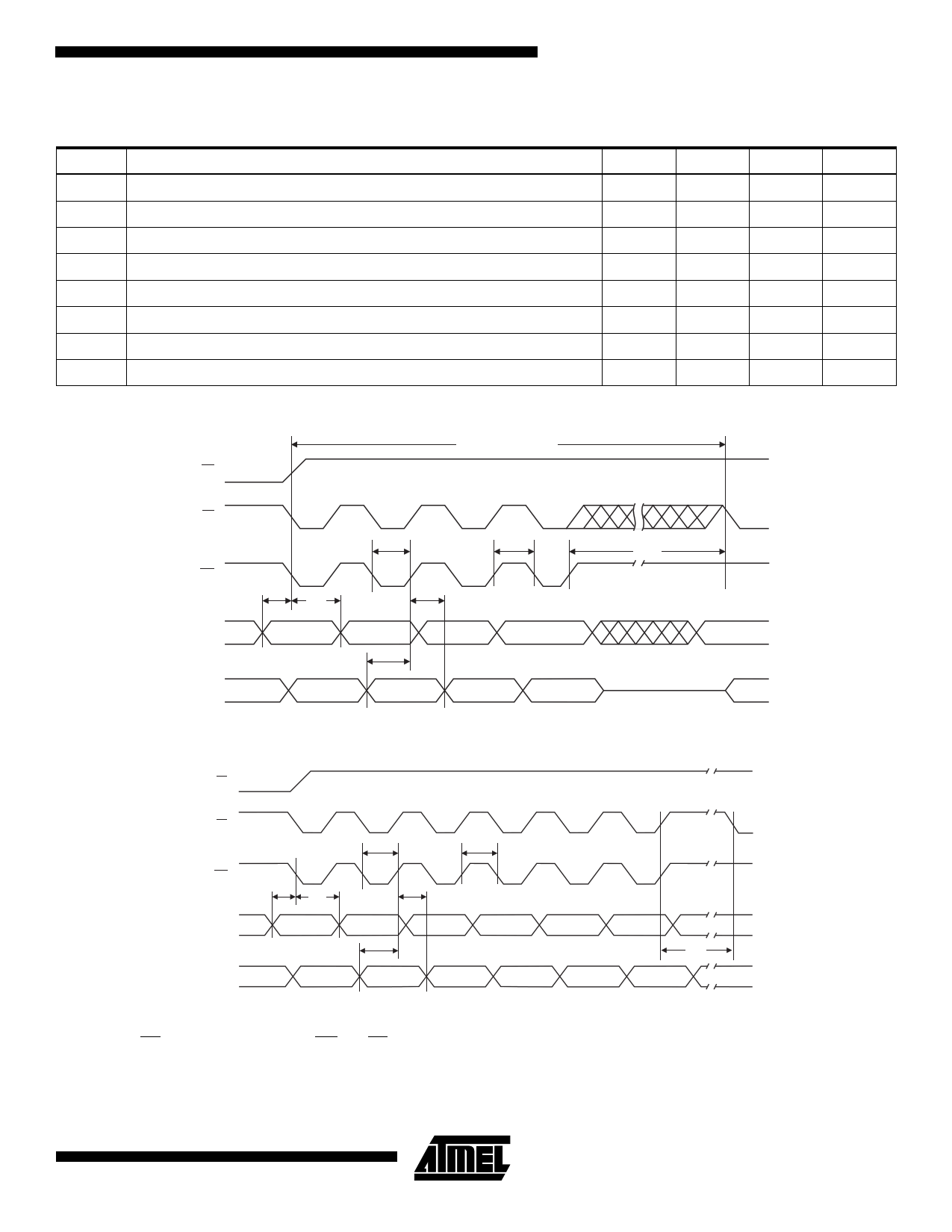
Program Cycle Characteristics
Symbol
tBP
tAS
tAH
tDS
tDH
tWP
tWPH
tEC
Parameter
Byte/Word Programming Time
Address Set-up Time
Address Hold Time
Data Set-up Time
Data Hold Time
Write Pulse Width
Write Pulse Width High
Erase Cycle Time
Program Cycle Waveforms
OE
PROGRAM CYCLE
Min Typ Max Units
30 µs
0 ns
100 ns
100 ns
0 ns
100 ns
50 ns
10 seconds
CE
WE
A0-A18
tAS
DATA
t WP
tAH tDH
5555
2AAA
t DS
AA 55
t WPH
5555
ADDRESS
A0 INPUT DATA
t BP
5555
AA
Sector or Chip Erase Cycle Waveforms
(1)
OE
CE
WE
A0-A18
DATA
t WP
t WPH
t AS tAH
t DH
5555
2AAA
t DS
5555
5555
2AAA
Note 2
t EC
AA
BYTE/
WORD 0
55
BYTE/
WORD 1
80
BYTE/
WORD 2
AA
BYTE/
WORD 3
55
BYTE/
WORD 4
Note 3
BYTE/
WORD 5
Notes: 1. OE must be high only when WE and CE are both low.
2. For chip erase, the address should be 5555. For sector erase, the address depends on what sector is to be erased.
(See note 4 under command definitions.)
3. For chip erase, the data should be 10H, and for sector erase, the data should be 30H.
11
11 Page | ||
| Páginas | Total 16 Páginas | |
| PDF Descargar | [ Datasheet AT49BV8192AT-20TC.PDF ] | |
Hoja de datos destacado
| Número de pieza | Descripción | Fabricantes |
| AT49BV8192AT-20TC | 8-Megabit 1M x 8/ 512K x 16 CMOS Flash Memory | ATMEL Corporation |
| AT49BV8192AT-20TI | 8-Megabit 1M x 8/ 512K x 16 CMOS Flash Memory | ATMEL Corporation |
| Número de pieza | Descripción | Fabricantes |
| SLA6805M | High Voltage 3 phase Motor Driver IC. |
Sanken |
| SDC1742 | 12- and 14-Bit Hybrid Synchro / Resolver-to-Digital Converters. |
Analog Devices |
|
DataSheet.es es una pagina web que funciona como un repositorio de manuales o hoja de datos de muchos de los productos más populares, |
| DataSheet.es | 2020 | Privacy Policy | Contacto | Buscar |
