|
|
|
PDF AT49LV001T-90PI Data sheet ( Hoja de datos )
| Número de pieza | AT49LV001T-90PI | |
| Descripción | 1-Megabit 128K x 8 Single 2.7-Volt Battery-Voltage Flash Memory | |
| Fabricantes | ATMEL Corporation | |
| Logotipo | ||
Hay una vista previa y un enlace de descarga de AT49LV001T-90PI (archivo pdf) en la parte inferior de esta página. Total 20 Páginas | ||
|
No Preview Available !
Features
• Single Supply for Read and Write: 2.7V to 3.6 (BV), 3.0 to 3.6V (LV)
• Fast Read Access Time - 70 ns
• Internal Program Control and Timer
• Sector Architecture
– One 16K Byte Boot Block with Programming Lockout
– Two 8K Byte Parameter Blocks
– Two Main Memory Blocks (32K, 64K) Bytes
• Fast Erase Cycle Time - 10 seconds
• Byte By Byte Programming - 30 µs/Byte Typical
• Hardware Data Protection
• DATA Polling For End Of Program Detection
• Low Power Dissipation
– 25 mA Active Current
– 50 µA CMOS Standby Current
• Typical 10,000 Write Cycles
Description
The AT49BV/LV001(N)(T) is a 3-volt-only in-system reprogrammable Flash Memory.
Its 1 megabit of memory is organized as 131,072 words by 8 bits. Manufactured with
Atmel’s advanced nonvolatile CMOS technology, the device offers access times to 70
ns with power dissipation of just 90 mW over the commercial temperature range.
When the device is deselected, the CMOS standby current is less than 50 µA. For the
(continued)
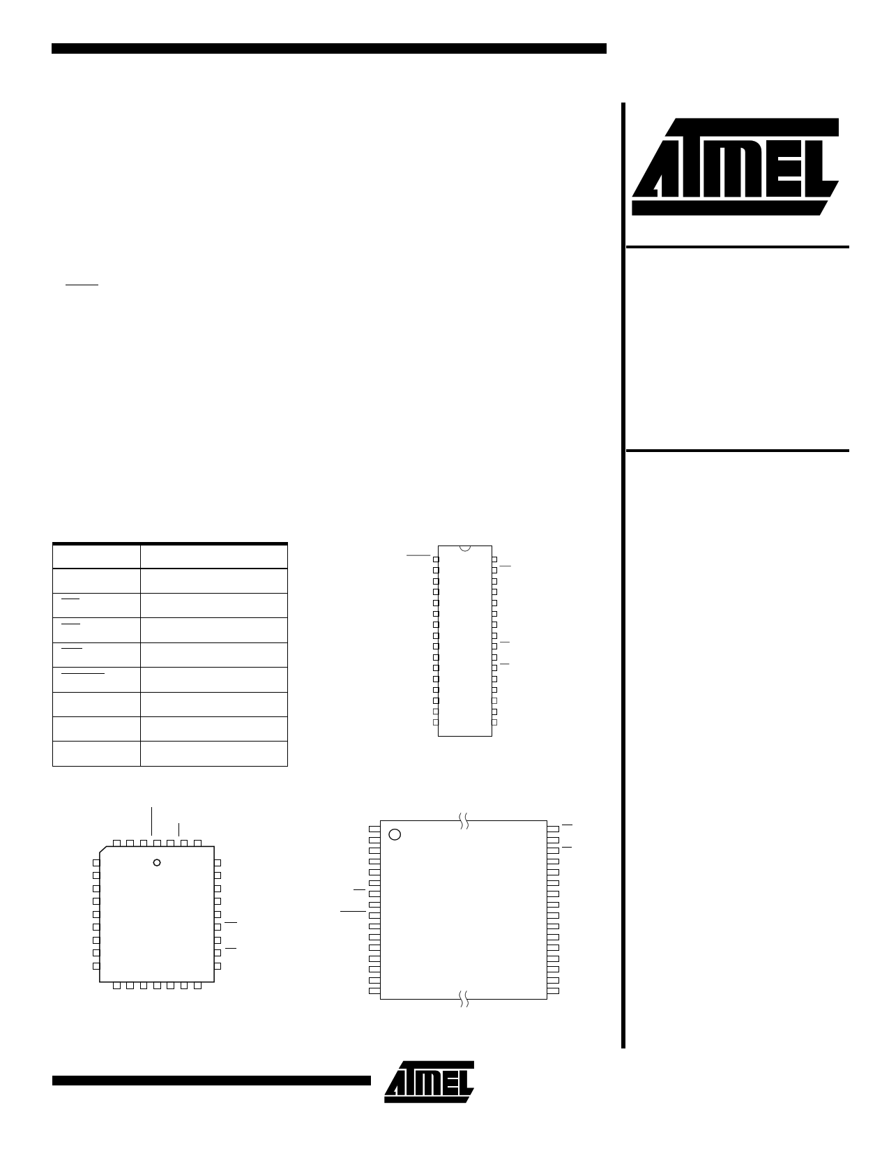
Pin Configurations
DIP Top View
Pin Name
A0 - A16
CE
OE
WE
RESET
I/O0 - I/O7
DC
NC
Function
Addresses
Chip Enable
Output Enable
Write Enable
RESET
Data Inputs/Outputs
Don’t Connect
No Connect
PLCC Top View
*RESET
A16
A15
A12
A7
A6
A5
A4
A3
A2
A1
A0
I/O0
I/O1
I/O2
GND
1
2
3
4
5
6
7
8
9
10
11
12
13
14
15
16
32 VCC
31 WE
30 NC
29 A14
28 A13
27 A8
26 A9
25 A11
24 OE
23 A10
22 CE
21 I/O7
20 I/O6
19 I/O5
18 I/O4
17 I/O3
VSOP Top View (8 x 14mm) or
TSOP Top View (8 x 20mm)
Type 1
A7
A6
A5
A4
A3
A2
A1
A0
I/O0
5
6
7
8
9
10
11
12
13
29 A14
28 A13
27 A8
26 A9
25 A11
24 OE
23 A10
22 CE
21 I/O7
A11
A9
A8
A13
A14
NC
WE
VCC
*RESET
A16
A15
A12
A7
A6
A5
A4
1
2
3
4
5
6
7
8
9
10
11
12
13
14
15
16
32 OE
31 A10
30 CE
29 I/O7
28 I/O6
27 I/O5
26 I/O4
25 I/O3
24 GND
23 I/O2
22 I/O1
21 I/O0
20 A0
19 A1
18 A2
17 A3
*Note: This pin is a DC on the AT49BV001N(T) and AT49LV001N(T).
1-Megabit
(128K x 8)
Single 2.7-Volt
Battery-Voltage™
Flash Memory
AT49BV001
AT49LV001
AT49BV001N
AT49LV001N
AT49BV001T
AT49LV001T
AT49BV001NT
AT49LV001NT
Rev. 1110A–07/98
1
1 page 
AT49BV/LV001(N)(T)
Command Definition (in Hex)(1)
Command
Sequence
Bus
Cycles
1st Bus
Cycle
Addr Data
2nd Bus
Cycle
Addr Data
3rd Bus
Cycle
Addr Data
4th Bus
Cycle
Addr Data
5th Bus
Cycle
Addr Data
Read
Chip Erase
1 Addr DOUT
6 5555 AA 2AAA 55 5555 80 5555 AA 2AAA 55
Sector Erase
6 5555 AA 2AAA 55 5555 80 5555 AA 2AAA 55
Byte Program
4 5555 AA 2AAA 55 5555 A0 Addr DIN
Boot Block Lockout(2) 6 5555 AA 2AAA 55 5555 80 5555 AA 2AAA 55
Product ID Entry
3 5555 AA 2AAA 55 5555 90
Product ID Exit(3)
3 5555 AA 2AAA 55 5555 F0
Product ID Exit(3)
1 XXXX F0
Notes: 1. The DATA FORMAT in each bus cycle is as follows: I/O7 - I/O0 (Hex)
2. The 16K byte boot sector has the address range 00000H to 03FFFH for the AT49BV/LV001(N) and
1C000H to 1FFFFH for the AT49BV/LV001(N)T.
3. Either one of the Product ID Exit commands can be used.
4. SA = sector addresses:
For the AT49BV/LV001(N):
SA = 10000 to 1FFFF for BOOT BLOCK
Nothing will happen and the device goes back to the read mode in 100 ns
SA = 04000 to 05FFF for PARAMETER BLOCK 1
SA = 06000 to 07FFF for PARAMETER BLOCK 2
SA = 08000 to 0FFFF for MAIN MEMORY ARRAY BLOCK 1
This command will erase - PB1, PB2 and MMB1
SA = 10000 to 1FFFF for MAIN MEMORY ARRAY BLOCK 2
6th Bus
Cycle
Addr Data
5555
SA(4)
10
30
5555 40
For the AT49BV/LV001(N)T:
SA = 1C000 to 1FFFF for BOOT BLOCK
Nothing will happen and the device goes back to the read mode in 100 ns
SA = 1A000 to 1BFFF for PARAMETER BLOCK 1
SA = 18000 to 19FFF for PARAMETER BLOCK 2
SA = 10000 to 17FFF for MAIN MEMORY ARRAY BLOCK 1
This command will erase - PB1, PB2 and MMB1
SA = 00000 to 0FFFF for MAIN MEMORY ARRAY BLOCK 2
Absolute Maximum Ratings*
Temperature Under Bias ................................ -55°C to +125°C
Storage Temperature ..................................... -65°C to +150°C
All Input Voltages
(including NC Pins)
with Respect to Ground ...................................-0.6V to +6.25V
All Output Voltages
with Respect to Ground .............................-0.6V to VCC + 0.6V
Voltage on OE
with Respect to Ground ...................................-0.6V to +13.5V
*NOTICE:
Stresses beyond those listed under “Absolute Maxi-
mum Ratings” may cause permanent damage to the
device. This is a stress rating only and functional
operation of the device at these or any other condi-
tions beyond those indicated in the operational sec-
tions of this specification is not implied. Exposure to
absolute maximum rating conditions for extended
periods may affect device reliability.
5
5 Page 
AT49BV/LV001(N)(T)
Software Product
Identification Entry(1)
LOAD DATA AA
TO
ADDRESS 5555
LOAD DATA 55
TO
ADDRESS 2AAA
LOAD DATA 90
TO
ADDRESS 5555
ENTER PRODUCT
IDENTIFICATION
MODE(2)(3)(5)
Software Product
Identification Exit(1)
LOAD DATA AA
TO
ADDRESS 5555
OR
LOAD DATA F0
TO
ANY ADDRESS
LOAD DATA 55
TO
ADDRESS 2AAA
EXIT PRODUCT
IDENTIFICATION
MODE(4)
LOAD DATA F0
TO
ADDRESS 5555
EXIT PRODUCT
IDENTIFICATION
MODE(4)
Notes for software product identification
1. Data Format: I/O7 - I/O0 (Hex);
Address Format: A14 - A0 (Hex).
2. A1 - A16 = VIL.
Manufacture Code is read for A0 = VIL;
Device Code is read for A0 = VIH.
3. The device does not remain in identification mode if
powered down.
4. The device returns to standard operation mode.
5. Manufacturer Code: 1FH
Device Code: 05H - AT49BV/LV001(N)
04H - AT49BV/LV001(N)T
Boot Block Lockout
Feature Enable Algorithm(1)
LOAD DATA AA
TO
ADDRESS 5555
LOAD DATA 55
TO
ADDRESS 2AAA
LOAD DATA 80
TO
ADDRESS 5555
LOAD DATA AA
TO
ADDRESS 5555
LOAD DATA 55
TO
ADDRESS 2AAA
LOAD DATA 40
TO
ADDRESS 5555
PAUSE 1 second(2)
Notes for boot block lockout feature enable:
1. Data Format: I/O7 - I/O0 (Hex);
Address Format: A14 - A0 (Hex).
2. Boot block lockout feature enabled.
11
11 Page | ||
| Páginas | Total 20 Páginas | |
| PDF Descargar | [ Datasheet AT49LV001T-90PI.PDF ] | |
Hoja de datos destacado
| Número de pieza | Descripción | Fabricantes |
| AT49LV001T-90PC | 1-Megabit 128K x 8 Single 2.7-Volt Battery-Voltage Flash Memory | ATMEL Corporation |
| AT49LV001T-90PI | 1-Megabit 128K x 8 Single 2.7-Volt Battery-Voltage Flash Memory | ATMEL Corporation |
| Número de pieza | Descripción | Fabricantes |
| SLA6805M | High Voltage 3 phase Motor Driver IC. |
Sanken |
| SDC1742 | 12- and 14-Bit Hybrid Synchro / Resolver-to-Digital Converters. |
Analog Devices |
|
DataSheet.es es una pagina web que funciona como un repositorio de manuales o hoja de datos de muchos de los productos más populares, |
| DataSheet.es | 2020 | Privacy Policy | Contacto | Buscar |