|
|
|
PDF AD621 Data sheet ( Hoja de datos )
| Número de pieza | AD621 | |
| Descripción | Low Drift/ Low Power Instrumentation Amplifier | |
| Fabricantes | Analog Devices | |
| Logotipo | ||
Hay una vista previa y un enlace de descarga de AD621 (archivo pdf) en la parte inferior de esta página. Total 16 Páginas | ||
|
No Preview Available !
a
Low Drift, Low Power
Instrumentation Amplifier
AD621
FEATURES
EASY TO USE
Pin-Strappable Gains of 10 & 100
All Errors Specified for Total System Performance
Higher Performance than Discrete In-Amp Designs
Available in 8-Pin DIP and SOIC
Low Power, 1.3 mA max Supply Current
Wide Power Supply Range (؎2.3 V to ؎18 V)
EXCELLENT DC PERFORMANCE
0.15% max, Total Gain Error
؎5 ppm/؇C, Total Gain Drift
125 V max, Total Offset Voltage
1.0 V/؇C max, Offset Voltage Drift
LOW NOISE
9 nV/√Hz, @ 1 kHz, Input Voltage Noise
0.28 V p-p Noise (0.1 Hz to 10 Hz}
EXCELLENT AC SPECIFICATIONS
800 kHz Bandwidth (G = 10}, 200 kHz (G = 100}
12 s Settling Time to 0.01%
APPLICATIONS
Weigh Scales
Transducer Interface & Data Acquisition Systems
Industrial Process Controls
Battery Powered and Portable Equipment
PRODUCT DESCRIPTION
The AD621 is an easy to use, low cost, low power, high accu-
racy instrumentation amplifier which is ideally suited for a wide
range of applications. Its unique combination of high perfor-
mance, small size and low power, outperforms discrete in amp
implementations. High functionality, low gain errors and low
gain drift errors are achieved by the use of internal gain setting
resistors. Fixed gains of 10 and 100 can be easily set via external
30,000
25,000
20,000
15,000
10,000
5,000
AD621A
3 - OP AMP
IN-AMPS
(3 OP 07'S)
0
5 10 15 20
SUPPLY CURRENT – mA
Three Op Amp IA Designs vs. AD621
REV. A
Information furnished by Analog Devices is believed to be accurate and
reliable. However, no responsibility is assumed by Analog Devices for its
use, nor for any infringements of patents or other rights of third parties
which may result from its use. No license is granted by implication or
otherwise under any patent or patent rights of Analog Devices.
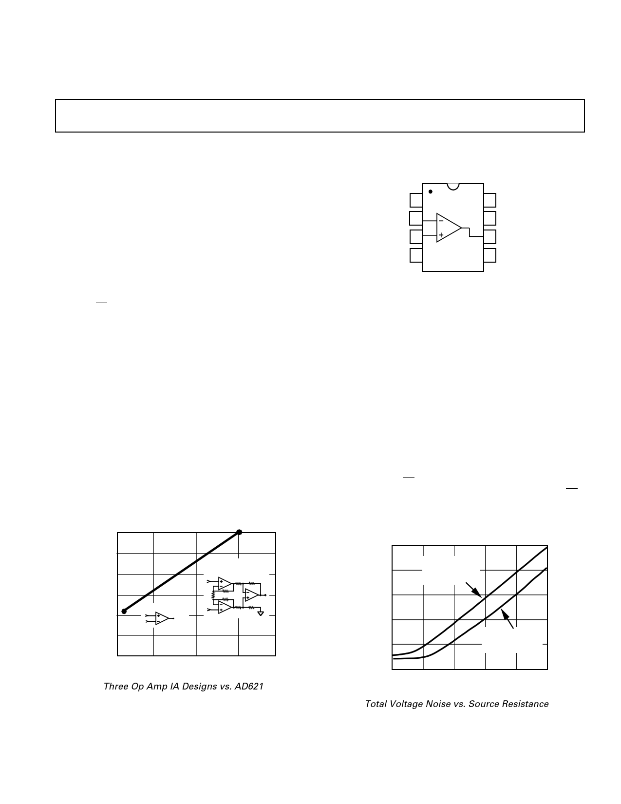
CONNECTION DIAGRAM
8-Pin Plastic Mini-DIP (N), Cerdip (Q)
and SOIC (R) Packages
G=10/100 1
–IN 2
AD621
8 G=10/100
7 +VS
+IN 3
6 OUTPUT
–VS 4
TOP VIEW
5 REF
pin strapping. The AD621 is fully specified as a total system,
therefore, simplifying the design process.
For portable or remote applications, where power dissipation,
size and weight are critical, the AD621 features a very low sup-
ply current of 1.3 mA max and is packaged in a compact 8-pin
SOIC, 8-pin plastic DIP or 8-pin cerdip. The AD621 also
excels in applications requiring high total accuracy, such as pre-
cision data acquisition systems used in weigh scales and trans-
ducer interface circuits. Low maximum error specifications
including nonlinearity of 10 ppm, gain drift of 5 ppm/°C, 50 µV
offset voltage and 0.6 µV/°C offset drift (“B” grade), make pos-
sible total system performance at a lower cost than has been pre-
viously achieved with discrete designs or with other monolithic
instrumentation amplifiers.
When operating from high source impedances, as in ECG and
blood pressure monitors, the AD621 features the ideal combina-
tion of low noise and low input bias currents. Voltage noise is
specified as 9 nV/√Hz at 1 kHz and 0.28 µV p-p from 0.1 Hz to
10 Hz. Input current noise is also extremely low at 0.1 pA/√Hz.
The AD621 outperforms FET input devices with an input bias
current specification of 1.5 nA max over the full industrial tem-
perature range.
10,000
1,000
100
TYPICAL STANDARD
BIPOLAR INPUT
IN-AMP
10
AD621 SUPERßETA
1 BIPOLAR INPUT
IN-AMP
0.1
1k
10k 100k
1M
SOURCE RESISTANCE – Ω
10M
100M
Total Voltage Noise vs. Source Resistance
One Technology Way, P.O. Box 9106, Norwood, MA 02062-9106, U.S.A.
Tel: 617/329-4700
Fax: 617/326-8703
1 page 
50
SAMPLE SIZE = 90
40
30
20
10
0
–200
–100 0 +100
INPUT OFFSET VOLTAGE – µV
+200
Figure 1. Typical Distribution of VOS, Gain = 10
50
SAMPLE SIZE = 90
40
30
20
10
0
–80
–40 0 +40
INPUT OFFSET VOLTAGE – µV
+80
Figure 2. Typical Distribution of VOS, Gain = 100
50
SAMPLE SIZE = 90
40
30
20
10
0
–400
–200 0 +200
INPUT OFFSET CURRENT – pA
+400
Figure 3. Typical Distribution of Input Offset Current
Typical Characteristics–AD621
50
SAMPLE SIZE = 90
40
30
20
10
0
–800
–400 0 +400
INPUT BIAS CURRENT – pA
+800
Figure 4. Typical Distribution of Input Bias Current
2
1.5
1
0.5
0
012345
WARM-UP TIME – Minutes
Figure 5. Change in Input Offset Voltage vs. Warm-Up Time
1000
100
GAIN = 10
10
GAIN = 100
1
1 10 100 1k 10k 100k
FREQUENCY – Hz
Figure 6. Voltage Noise Spectral Density
REV. A
–5–
5 Page 
+5V
3kΩ 3kΩ
3kΩ 3kΩ
1.7mA
AD621
37
20kΩ
8
AD621B
6
1 5 10kΩ
24
1.3mA
MAX
0.10mA
20kΩ
AD705
0.6mA
MAX
REF
IN
ADC
AGND
DIGITAL
DATA
OUTPUT
Figure 31. A Pressure Monitor Circuit which Operates on a +5 V Power Supply
Pressure Measurement
Although useful in many bridge applications such as weigh-
scales, the AD621 is especially suited for higher resistance pres-
sure sensors powered at lower voltages where small size and low
power become more even significant.
Figure 31 shows a 3 kΩ pressure transducer bridge powered
from +5 V. In such a circuit, the bridge consumes only 1.7 mA.
Adding the AD621 and a buffered voltage divider allows the sig-
nal to be conditioned for only 3.8 mA of total supply current.
Small size and low cost make the AD621 especially attractive for
voltage output pressure transducers. Since it delivers low noise
and drift, it will also serve applications such as diagnostic
noninvasion blood pressure measurement.
Wide Dynamic Range Gain Block Suppresses Large Common-
Mode and Offset Signals
The AD621 is especially useful in wide dynamic range applica-
tions such as those requiring the amplification of signals in the
presence of large, unwanted common-mode signals or offsets.
Many monolithic in amps achieve low total input drift and noise
errors only at relatively high gains (~100). In contrast the
AD621’s low output errors allow such performance at a gain of
10, thus allowing larger input signals and therefore greater
dynamic range. The circuit of Figure 32 (± 15 V supply, G = 10)
has only 2.5 µV/°C max. VOS drift and 0.55 µ/V p-p typical
0.1 Hz to 10 Hz noise, yet will amplify a ± 0.5 V differential sig-
nal while suppressing a ± 10 V common-mode signal, or it will
amplify a ± 1.25 V differential signal while suppressing a 1 V
offset by use of the DAC driving the reference pin of the
AD621. An added benefit, the offsetting DAC connected to the
reference pin allows removal of a dc signal without the associ-
ated time-constant of ac coupling. Note the representations of a
differential and common-mode signal shown in Figure 32 such
that a single-ended (or normal mode) signal of +1 V would be
composed of a +0.5 V common-mode component and a +1 V
differential component.
Table I. Make vs. Buy Error Budget
Error Source
AD621 Circuit
Calculation
Discrete Circuit
Calculation
Error, ppm of Full Scale
AD621
Discrete
ABSOLUTE ACCURACY at TA = +25°C
Input Offset Voltage, µV
Output Offset Voltage, µV
Input Offset Current, nA
CMR, dB
125 µV/20 mV
N/A
2 nA × 350 Ω/20 mV
110 dB→3.16 ppm, × 5 V/20 mV
(150 µV × 2/20 mV
((150 µV × 2)/100)/20 mV
(6 nA × 350 Ω)/20 mV
(0.02% Match × 5 V)/20 mV
DRIFT TO +85°C
Gain Drift, ppm/°C
Input Offset Voltage Drift, µV/°C
Output Offset Voltage Drift, µV/°C
5 ppm × 60°C
1 µV/°C × 60°C/20 mV
N/A
Total Absolute Error
100 ppm/°C Track × 60°C
(2.5 µV/°C × 2 × 60°C)/20 mV
(2.5 µV/°C × 2 × 60°C)/100/20 mV
16,250
N/A
12,118
12,791
17,558
13,300
13,000
N/A
15,000
12,150
121,53
14,988
20,191
12,600
15,000
12,150
RESOLUTION
Gain Nonlinearity, ppm of Full Scale
40 ppm
Typ 0.1 Hz–10 Hz Voltage Noise, µV p-p 0.28 µV p-p/20 mV
Total Drift Error
40 ppm
(0.38 µV p-p × √2)120 mV
13,690
12,140
121,14
15,750
12,140
12,127
G = 100, VS = ± 15 V.
(All errors are min/max and referred to input.)
Total Resolution Error
Grand Total Error
121,54
11,472
121,67
36,008
REV. A
–11–
11 Page | ||
| Páginas | Total 16 Páginas | |
| PDF Descargar | [ Datasheet AD621.PDF ] | |
Hoja de datos destacado
| Número de pieza | Descripción | Fabricantes |
| AD620 | Low Power Instrumentation Amplifier | Analog Devices |
| AD621 | Low Drift/ Low Power Instrumentation Amplifier | Analog Devices |
| AD622 | Low Cost Instrumentation Amplifier | Analog Devices |
| AD623 | Low Cost Instrumentation Amplifier | Analog Devices |
| Número de pieza | Descripción | Fabricantes |
| SLA6805M | High Voltage 3 phase Motor Driver IC. |
Sanken |
| SDC1742 | 12- and 14-Bit Hybrid Synchro / Resolver-to-Digital Converters. |
Analog Devices |
|
DataSheet.es es una pagina web que funciona como un repositorio de manuales o hoja de datos de muchos de los productos más populares, |
| DataSheet.es | 2020 | Privacy Policy | Contacto | Buscar |