|
|
PDF AD6402 Data sheet ( Hoja de datos )
| Número de pieza | AD6402 | |
| Descripción | IF Transceiver Subsystem | |
| Fabricantes | Analog Devices | |
| Logotipo |  |
|
Hay una vista previa y un enlace de descarga de AD6402 (archivo pdf) en la parte inferior de esta página. Total 8 Páginas | ||
|
No Preview Available !
a
IF Transceiver Subsystem
AD6402
FEATURES
On-Chip Regulator
PLL Demodulator
On-Chip VCO
No Trims
Excellent Sensitivity
28-Lead SSOP Package
APPLICATIONS
DECT/PWT/WLAN
TDMA FM/FSK Systems
GENERAL DESCRIPTION
The AD6402 is a complete transceiver subsystem for use in
high bit rate radio systems employing FM or FSK modulation.
It is optimized for use in time domain multiple access (TDMA)
systems with communications rates of approximately 1 MBPS.
The AD6402 integrates key functions, including VCOs and a
low drop-out voltage regulator. The AD6402 operates directly
from an unregulated battery supply of 3.1 V to 4.5 V and pro-
vides a regulated voltage output which can be used for VCO
supply regulation on a companion RF chip such as the AD6401.
The AD6402 transceiver consists of a mixer, integrated IF
bandpass filter, IF limiter with RSSI detection, VCO, PLL
demodulator and a low dropout voltage regulator. On receive, it
downconverts an IF signal in the 110 MHz range to a second
IF frequency, this frequency being determined by the demodu-
lator reference divide ratios. It then filters, amplifies, and de-
modulates this signal. The AD6402 provides a filtered baseband
FUNCTIONAL BLOCK DIAGRAM
IFIN
TXOUT
TXOUTB
VCO
LIMITER/FILTER
PLL
DEMOD
2
AD6402
IF
VCO
VOLTAGE
REGULATOR
MODE
CONTROL
VREF
1
DC
OFFSET
COMP
RSSI
CFILT
DOUT
DFILP
PLLOUT
REFSEL
COFF
REFIN
FMMOD2
FMMOD1
VREG VBATT SLREF CTL1...3
MODOUT
data output. On transmit, it accepts a Gaussian Frequency Shift
Keying (GFSK) baseband signal, low-pass filters the signal if
required using the on-chip op amp and modulates the IF VCO
by varying the bias voltage on an off-chip varactor diode used in
the tank circuit.
The AD6402 has multiple power-down modes to maximize
battery life. It operates over a temperature range of –25°C to
+85°C and is packaged in a JEDEC standard 28-lead small-
shrink outline (SSOP) surface-mount package.
REV. 0
Information furnished by Analog Devices is believed to be accurate and
reliable. However, no responsibility is assumed by Analog Devices for its
use, nor for any infringements of patents or other rights of third parties
which may result from its use. No license is granted by implication or
otherwise under any patent or patent rights of Analog Devices.
One Technology Way, P.O. Box 9106, Norwood, MA 02062-9106, U.S.A.
Tel: 617/329-4700 World Wide Web Site: http://www.analog.com
Fax: 617/326-8703
© Analog Devices, Inc., 1997
1 page 
AD6402
Table I. Power Management Functionality
PLL PLL PLL
TL1
CTL2 CTL3 BIAS LOCK DMOD REF
REG
RX
VCO
MODE
0
0
0
–
–
–
OFF
OFF
–
–
SLEEP
0
0
1
–
–
–
OFF
ON
–
–
STANDBY
0
1
0
ON
ON
OFF
ON
ON
OFF
ON
RXLOCK
1
X0
ON
OFF
ON
ON
ON
ON
ON
RXDMOD
1
0
1
OFF OFF OFF ON
ON
OFF
ON
TRANSMIT
1
1
1
ON
ON
OFF
ON
ON
ON
ON
RXLOCKP
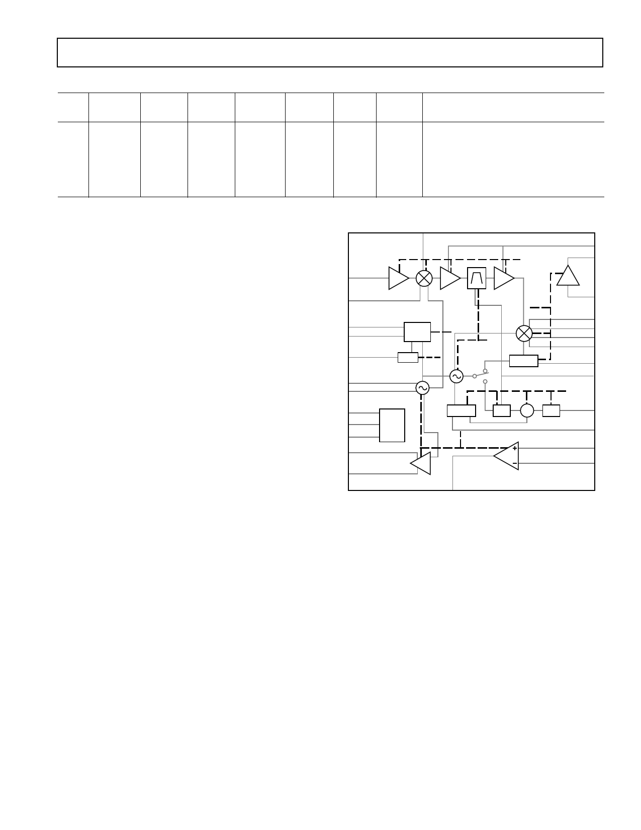
The AD6402 has six operating modes: SLEEP, STANDBY,
RXLOCK, RXDMOD, TRANSMIT and RXLOCKP. These
are summarized in Table I. The blocks referred to in Table I are
shown also in Figure 4. These modes are described as follows:
SLEEP:
The entire device is shut down.
STANDBY: All functions except the regulator are shut down.
RXLOCK:
The device locks to a local reference clock using
the lock PLL. The lock charge pump and divid-
ers are powered up. The VCO is also powered up.
RXDMOD: In this mode the lock charge pump and loop
dividers are shut down. The receive mixer, IF strip,
reference and demodulator are powered up.
TRANSMIT: This mode enables the VCO and transmit op
amp. The reference and regulator are also enabled.
RXLOCKP:
This mode may be used in a “prior to” timeslot,
i.e., the slot before the actual active receive
timeslot. In this mode, after lock has been
achieved in the RXLOCK mode, the receive
mixer, VCO and IF strip may then be indepen-
dently powered up from the demodulator loop.
This can result is power savings, since the de-
modulator may be powered down during the
IF VCO lock acquisition time.
IFIN
IFGND
VBAT
VREG
SLREF
VCO
VCOGND
CTL3
CTL2
CTL1
TXOUT
TXOUTB
IFVCC1
IFVCC2
RX
RSSI
DOUT
PLL DMOD
DFLIP
REG
REG
REF
REF
PLL BIAS
PLLOUT
PLLVCC
PLLGND
REXT
CP CFILT
COFF
PLL LOCK
/3,/5
CP PD /2
REFIN
VCO
REFSEL
FMMOD2
FMMOD1
MODOUT
Figure 2. Power Management Scheme
REV. 0
–5–
5 Page | ||
| Páginas | Total 8 Páginas | |
| PDF Descargar | [ Datasheet AD6402.PDF ] | |
Hoja de datos destacado
| Número de pieza | Descripción | Fabricantes |
| AD640 | DC-Coupled Demodulating 120 MHz Logarithmic Amplifier | Analog Devices |
| AD6402 | IF Transceiver Subsystem | Analog Devices |
| Número de pieza | Descripción | Fabricantes |
| SLA6805M | High Voltage 3 phase Motor Driver IC. |
Sanken |
| SDC1742 | 12- and 14-Bit Hybrid Synchro / Resolver-to-Digital Converters. |
Analog Devices |
|
DataSheet.es es una pagina web que funciona como un repositorio de manuales o hoja de datos de muchos de los productos más populares, |
| DataSheet.es | 2020 | Privacy Policy | Contacto | Buscar |
