|
|
|
PDF AD6635 Data sheet ( Hoja de datos )
| Número de pieza | AD6635 | |
| Descripción | 4-Channel/ 80 MSPS WCDMA Receive Signal Processor (RSP) | |
| Fabricantes | Analog Devices | |
| Logotipo | ||
Hay una vista previa y un enlace de descarga de AD6635 (archivo pdf) en la parte inferior de esta página. Total 30 Páginas | ||
|
No Preview Available !
4-Channel, 80 MSPS WCDMA
Receive Signal Processor (RSP)
AD6635
FEATURES
Four 80 MSPS Wideband Inputs (14 Linear Bits Plus 3 RSSI)
4 Real Input Ports/2 Complex Input Ports
Processes 4 Wideband Channels (UMTS or cdma2000
1x) or 8 GSM/EDGE, IS136 Channels
8 Independent Digital Receivers in a Single Package
Four 16-Bit Parallel Output Ports and Four 8-Bit Link Ports
4 Programmable Digital AGC Loops with 96 dB Range
Digital Resampling for Noninteger Decimation Rates
Programmable Decimating FIR Filters
4 Interpolating Half-Band Filters
Flexible Control for Multicarrier and Phased Array
Programmable Attenuator Control for Clip Prevention and
External Gain Ranging via Level Indicator
3.3 V I/O, 2.5 V CMOS Core
User Configurable Built-in Self Test (BIST) Capability
APPLICATIONS
Multicarrier, Multimode Digital Receivers
GSM, IS136, EDGE, PHS, IS95, UMTS, cdma2000
Micro and Pico Cell Systems, Software Radios
Wireless Local Loop
Smart Antenna Systems
In-Building Wireless Telephony
INA[13:0]
EXPA[2:0]
IENA
LIA-A
LIA-B
INB[13:0]
EXPB[2:0]
IENB
LIB-A
LIB-B
I
N
P
U
T
M
A
T
R
I
X
INC[13:0]
EXPC[2:0]
IENC
LIB-A
LIB-B
IND[13:0]
EXPD[2:0]
IEND
LID-A
LID-B
SYNCA
SYNCB
SYNCC
SYNCD
I
N
P
U
T
M
A
T
R
I
X
EXTERNAL
SYNC.
CIRCUIT
FUNCTIONAL BLOCK DIAGRAM
NCO
NCO
NCO
rCIC2
RESAMPLER
CIC5
rCIC2
RESAMPLER
CIC5
rCIC2
RESAMPLER
CIC5
rCIC2
RESAMPLER
CIC5
NCO
NCO
NCO
NCO
rCIC2
RESAMPLER
CIC5
rCIC2
RESAMPLER
CIC5
rCIC2
RESAMPLER
CIC5
rCIC2
RESAMPLER
CIC5
NCO
CLK
RSP
CLK
RAM
COEFFICIENT
FILTER
CHANNEL 0
RAM
COEFFICIENT
FILTER
CHANNEL 1
RAM
COEFFICIENT
FILTER
CHANNEL 2
RAM
COEFFICIENT
FILTER
CHANNEL 3
RAM
COEFFICIENT
FILTER
CHANNEL 4
RAM
COEFFICIENT
FILTER
CHANNEL 5
RAM
COEFFICIENT
FILTER
CHANNEL 6
RAM
COEFFICIENT
FILTER
CHANNEL 7
BUILT-IN (BIST)
SELF-TEST CIRCUITRY
TO A AND B
OUTPUT
PORTS
RCF OUTPUTS
CHANNELS 0, 1, 2,3
TO A AND B
OUTPUT
PORTS
CH A INTERPOLATING
HALF-BAND FILTER,
INTERLEAVING & AGC
TO A AND B
OUTPUT
PORTS
CH B INTERPOLATING
HALF-BAND FILTER,
INTERLEAVING & AGC
TO A AND B
OUTPUT
PORTS
RCF OUTPUTS
CHANNELS 0, 1, 2,3
PORT A
LINK PORT
OR
PARALLEL
PORT
CH A AND B
OUTPUT MUX
CIRCUITRY
PORT B
LINK PORT
OR
PARALLEL
PORT
TO C AND D
OUTPUT
PORTS
RCF OUTPUTS
CHANNELS 4, 5, 6,7
TO C AND D
OUTPUT
PORTS
CH C INTERPOLATING
HALF-BAND FILTER,
INTERLEAVING & AGC
TO C AND D
OUTPUT
PORTS
CH D INTERPOLATING
HALF-BAND FILTER,
INTERLEAVING & AGC
TO C AND D
OUTPUT
PORTS
RCF OUTPUTS
CHANNELS 4, 5, 6,7
MICROPORT OR SERIAL
PORT CONTROL
PORT C
8-BIT DSP
LINK PORT
OR
16-BIT
PARALLEL
OUTPUT
CH C AND D
OUTPUT MUX
CIRCUITRY
PORT D
8-BIT DSP
LINK PORT
OR
16-BIT
PARALLEL
OUTPUT
REV. 0
Information furnished by Analog Devices is believed to be accurate and
reliable. However, no responsibility is assumed by Analog Devices for its
use, nor for any infringements of patents or other rights of third parties that
may result from its use. No license is granted by implication or otherwise
under any patent or patent rights of Analog Devices. Trademarks and
registered trademarks are the property of their respective companies.
One Technology Way, P.O. Box 9106, Norwood, MA 02062-9106, U.S.A.
Tel: 781/329-4700
www.analog.com
Fax: 781/326-8703 © 2003 Analog Devices, Inc. All rights reserved.
1 page 
AD6635
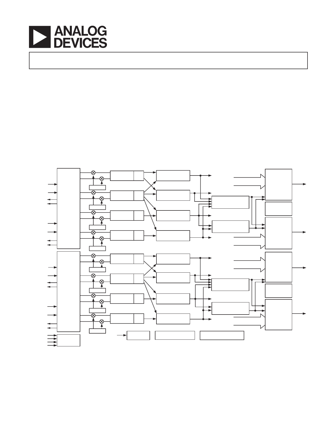
ARCHITECTURE
Each channel of the AD6635 has four signal processing stages:
a Frequency Translator, a second-order Resampling Cascaded
Integrator Comb FIR Filter (rCIC2), a fifth-order Cascaded
Integrator Comb FIR Filter (CIC5), and a RAM Coefficient
FIR Filter (RCF). Multiple modes are supported for clocking
data into and out of the chip, and for providing flexibility for inter-
facing to a wide variety of digitizers. Programming and control is
accomplished via serial and/or microprocessor interfaces.
Frequency translation is accomplished with a 32-bit complex
Numerically Controlled Oscillator (NCO). Real data entering
this stage is separated into inphase (I) and quadrature (Q) com-
ponents by multiplying with the complex NCO word. This stage
translates the input signal from a digital intermediate frequency
(IF) to digital baseband. Phase and amplitude dither may be
enabled on-chip to improve spurious performance of the NCO.
A phase-offset word is available to create a known phase rela-
tionship between multiple AD6635s or between channels.
Following frequency translation is a fixed coefficient, high speed,
second-order, Resampling Cascade Integrator Comb (rCIC2) filter
that reduces the sample rate based on the ratio between the deci-
mation and interpolation registers.
The next stage is a fifth-order Cascaded Integrator Comb (CIC5)
filter whose response is defined by the decimation rate. The pur-
pose of these filters is to reduce the data rate to the final filter stage
(RCF), so that it can calculate more taps for the same RCF band-
width. The CIC5 filter has better antialiasing (filtering) compared
to rCIC2. In light of this, the user is advised to use this filter only if
resampling is required or if the required decimation cannot be
handled by CIC5 alone.
The final stage is a sum-of-products FIR filter with program-
mable 20-bit coefficients, and decimation rates programmable
from 1 to 256 (1 to 32 in practice). The RAM Coefficient FIR
Filter (RCF) can handle a maximum of 160 taps.
The data coming out of the RCF can be sent to output ports or
to an interleaver. This section can interleave data from more
than one channel. One carrier can be processed using more than
one channel and the interleaver will interleave the data back into
the output section. This way, processing power from more than
one channel can be used for one carrier.
The interleaved data is sent into a fixed coefficient half-band
interpolation filter where data is interpolated by a factor of two.
Digital AGC following the half-band filter has a gain range of
96.3 dB. This AGC section is completely programmable in
terms of its response. Four each of half-band filters and AGCs
are present in the AD6635, as shown in the Functional Block
Diagram. These half-band filters and AGC sections can be
bypassed independent of each other.
The overall filter response for the AD6635 is the composite of
all decimating and interpolating stages. Each successive filter
stage is capable of narrower transition bandwidths, but requires
a greater number of CLK cycles to calculate the output. More
decimation in the first filter stage will minimize overall power
consumption. Each independent filter stage can be bypassed in
a unique way. Data from the chip is interfaced to the DSP via
either a high speed parallel port or a TigerSHARC compatible
link port. Each output can be independently configured to use
either the parallel port or the link port.
Figure 1 illustrates the tuning function of the AD6635 NCOs to
select and filter a single channel from a wide input spectrum.
The frequency translator “tunes” the desired carrier to base-
band. Figure 2 shows the combined filter response of the rCIC2,
CIC5, and RCF filters for a sample filter configuration.
REV. 0
–5–
5 Page 
AD6635
ABSOLUTE MAXIMUM RATINGS*
Supply Voltage . . . . . . . . . . . . . . . . . . . . . . . . . . . . . . . . . 3.6 V
Input Voltage . . . . . . . . . . . . . –0.3 V to +5.3 V (5 V Tolerant)
Output Voltage Swing . . . . . . . . . . . –0.3 V to VDDIO + 0.3 V
Load Capacitance . . . . . . . . . . . . . . . . . . . . . . . . . . . . . 200 pF
Junction Temperature Under Bias . . . . . . . . . . . . . . . . . 150∞C
Storage Temperature Range . . . . . . . . . . . . . –65∞C to +150∞C
Lead Temperature (5 sec) . . . . . . . . . . . . . . . . . . . . . . . 280∞C
*Stresses greater than those listed above may cause permanent damage to the device
These are stress ratings only; functional operation of the devices at these or any
other conditions greater than those indicated in the operational sections of this
specification is not implied. Exposure to absolute maximum rating conditions for
extended periods may affect device reliability.
Thermal Characteristics
324-Lead BGA:
JA = 16.87∞C/W, no airflow.
Thermal measurements made in the horizontal position on a
4-layer board.
EXPLANATION OF TEST LEVELS
I 100% Production Tested.
II 100% Production Tested at 25∞C, and Sample Tested at
Specified Temperatures.
III Sample Tested Only.
IV Parameter Guaranteed by Design and Analysis.
V Parameter is Typical Value Only.
VI 100% Production Tested at 25∞C, and Sample Tested at
Temperature Extremes.
Model
AD6635BB
AD6635BB/PCB
Temperature Range
–40ºC to +85ºC
ORDERING GUIDE
Package Descriptions
324-Lead PBGA (Ball Grid Array)
Evaluation Board with AD6635 and Software
Package Option
B-324
CAUTION
ESD (electrostatic discharge) sensitive device. Electrostatic charges as high as 4000 V readily
accumulate on the human body and test equipment and can discharge without detection. Although the
AD6635 features proprietary ESD protection circuitry, permanent damage may occur on devices
subjected to high energy electrostatic discharges. Therefore, proper ESD precautions are recommended
to avoid performance degradation or loss of functionality.
REV. 0
–11–
11 Page | ||
| Páginas | Total 30 Páginas | |
| PDF Descargar | [ Datasheet AD6635.PDF ] | |
Hoja de datos destacado
| Número de pieza | Descripción | Fabricantes |
| AD6630 | Differential/ Low Noise IF Gain Block with Output Clamping | Analog Devices |
| AD6633 | Multichannel Digital Upconverter | Analog Devices |
| AD6634 | 80 MSPS/ Dual-Channel WCDMA Receive Signal Processor (RSP) | Analog Devices |
| AD6635 | 4-Channel/ 80 MSPS WCDMA Receive Signal Processor (RSP) | Analog Devices |
| Número de pieza | Descripción | Fabricantes |
| SLA6805M | High Voltage 3 phase Motor Driver IC. |
Sanken |
| SDC1742 | 12- and 14-Bit Hybrid Synchro / Resolver-to-Digital Converters. |
Analog Devices |
|
DataSheet.es es una pagina web que funciona como un repositorio de manuales o hoja de datos de muchos de los productos más populares, |
| DataSheet.es | 2020 | Privacy Policy | Contacto | Buscar |