|
|
|
PDF AD6640 Data sheet ( Hoja de datos )
| Número de pieza | AD6640 | |
| Descripción | 12-Bit/ 65 MSPS IF Sampling A/D Converter | |
| Fabricantes | Analog Devices | |
| Logotipo | ||
Hay una vista previa y un enlace de descarga de AD6640 (archivo pdf) en la parte inferior de esta página. Total 24 Páginas | ||
|
No Preview Available !
a
FEATURES
65 MSPS Minimum Sample Rate
80 dB Spurious-Free Dynamic Range
IF-Sampling to 70 MHz
710 mW Power Dissipation
Single +5 V Supply
On-Chip T/H and Reference
Twos Complement Output Format
3.3 V or 5 V CMOS-Compatible Output Levels
APPLICATIONS
Cellular/PCS Base Stations
Multichannel, Multimode Receivers
GPS Anti-Jamming Receivers
Communications Receivers
Phased Array Receivers
12-Bit, 65 MSPS
IF Sampling A/D Converter
AD6640
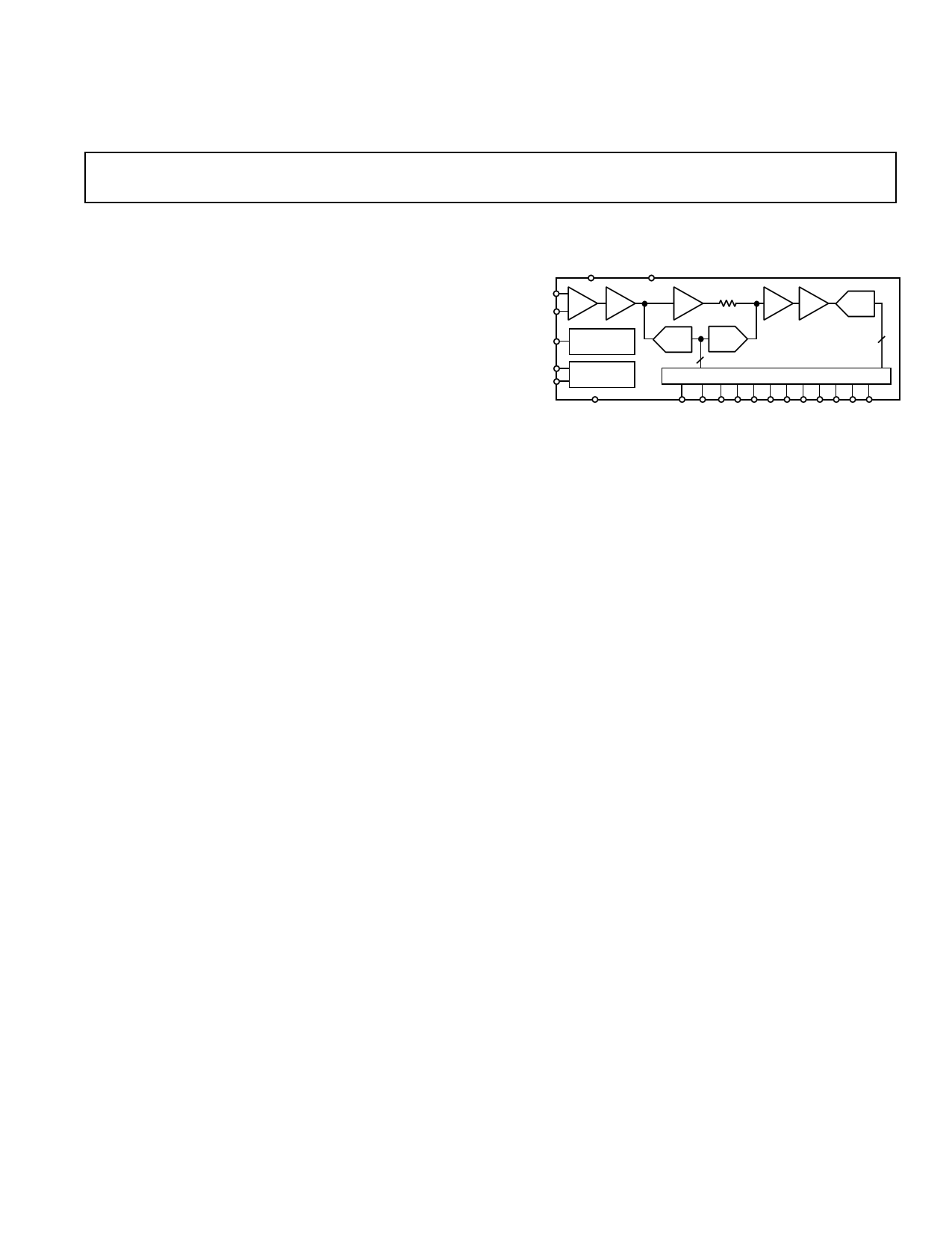
FUNCTIONAL BLOCK DIAGRAM
AIN
AIN
VREF
ENCODE
ENCODE
AVCC
DVCC
BUF TH1
TH2
TH3 A
ADC
+2.4V
REFERENCE
INTERNAL
TIMING
GND
ADC
DAC
AD6640
7
6
DIGITAL ERROR CORRECTION LOGIC
MSB
LSB
D11 D10 D9 D8 D7 D6 D5 D4 D3 D2 D1 D0
PRODUCT DESCRIPTION
The AD6640 is a high speed, high performance, low power,
monolithic 12-bit analog-to-digital converter. All necessary
functions, including track-and-hold (T/H) and reference are
included on-chip to provide a complete conversion solution.
The AD6640 runs on a single +5 V supply and provides CMOS-
compatible digital outputs at 65 MSPS.
Specifically designed to address the needs of multichannel,
multimode receivers, the AD6640 maintains 80 dB spurious-
free dynamic range (SFDR) over a bandwidth of 25 MHz.
Noise performance is also exceptional; typical signal-to-noise
ratio is 68 dB.
The AD6640 is built on Analog Devices’ high speed complemen-
tary bipolar process (XFCB) and uses an innovative multipass
architecture. Units are packaged in a 44-terminal Plastic Thin
Quad Flatpack (TQFP) specified from –40°C to +85°C.
PRODUCT HIGHLIGHTS
1. Guaranteed sample rate is 65 MSPS.
2. Fully differential analog input stage specified for frequencies
up to 70 MHz; enables “IF Sampling.”
3. Low power dissipation: 710 mW off a single +5 V supply.
4. Digital outputs may be run on +3.3 V supply for easy inter-
face to digital ASICs.
5. Complete Solution: reference and track-and-hold.
6. Packaged in small, surface mount, plastic 44-terminal TQFP.
REV. 0
Information furnished by Analog Devices is believed to be accurate and
reliable. However, no responsibility is assumed by Analog Devices for its
use, nor for any infringements of patents or other rights of third parties
which may result from its use. No license is granted by implication or
otherwise under any patent or patent rights of Analog Devices.
One Technology Way, P.O. Box 9106, Norwood, MA 02062-9106, U.S.A.
Tel: 781/329-4700 World Wide Web Site: http://www.analog.com
Fax: 781/326-8703
© Analog Devices, Inc., 1998
1 page 
Pin No.
1, 2, 36, 37, 40, 41
3
4
Name
DVCC
ENCODE
ENCODE
5, 6, 13, 14, 17, 18, 21,
22, 24, 34, 35, 38, 39
7
8
9
GND
AIN
AIN
VREF
10
11, 12, 15, 16, 19, 20
23
25
26–33
42, 43
44
C1
AVCC
NC
D0 (LSB)
D1–D8
D9–D10
D11 (MSB)1
NOTE
1Output coded as twos complement.
AD6640
PIN FUNCTION DESCRIPTIONS
Function
+3.3 V/+5 V Power Supply (Digital). Powers output stage only.
Encode Input. Data conversion initiated on rising edge.
Complement of ENCODE. Drive differentially with ENCODE or bypass to
Ground for single-ended clock mode. See Encoding the AD6640 section.
Ground.
Analog Input.
Complement of Analog Input.
Internal Voltage Reference. Nominally +2.4 V. Bypass to Ground with
0.1 µF + 0.01 µF microwave chip capacitor.
Internal Bias Point. Bypass to ground with 0.01 µF capacitor.
+5 V Power Supply (Analog).
No Connect.
Digital Output Bit (Least Significant Bit).
Digital Output Bits.
Digital Output Bits.
Digital Output Bit (Most Significant Bit).
PIN CONFIGURATION
44 43 42 41 40 39 38 37 36 35 34
DVCC 1
DVCC 2
ENCODE 3
ENCODE 4
GND 5
GND 6
AIN 7
AIN 8
VREF 9
C1 10
AVCC 11
PIN 1
AD6640
TOP VIEW
(Not to Scale)
33 D8
32 D7
31 D6
30 D5
29 D4
28 D3
27 D2
26 D1
25 D0 (LSB)
24 GND
23 NC
12 13 14 15 16 17 18 19 20 21 22
NC = NO CONNECT
REV. 0
–5–
5 Page 
AD6640
THEORY OF OPERATION
The AD6640 analog-to-digital converter (ADC) employs a two-
stage subrange architecture. This design approach ensures
12-bit accuracy, without the need for laser trim, at low power.
As shown in the functional block diagram, the AD6640 has
complementary analog input pins, AIN and AIN. Each analog
input is centered at 2.4 volts and should swing ± 0.5 volts
around this reference (ref. Figure 2). Since AIN and AIN are
180 degrees out of phase, the differential analog input signal is
2 volts peak-to-peak.
Both analog inputs are buffered prior to the first track-and-hold,
TH1. The high state of the ENCODE pulse places TH1 in
hold mode. The held value of TH1 is applied to the input of a
6-bit coarse ADC. The digital output of the coarse ADC drives
a 6-bit DAC; the DAC is 12 bits accurate. The output of the 6-
bit DAC is subtracted from the delayed analog signal at the
input of TH3 to generate a residue signal. TH2 is used as an
analog pipeline to null out the digital delay of the coarse ADC.
The 6-bit coarse ADC word and 7-bit residue word are added
together and corrected in the digital error correction logic to
generate the output word. The result is a 12-bit parallel digital
CMOS-compatible word, coded as twos complement.
APPLYING THE AD6640
Encoding the AD6640
Best performance is obtained by driving the encode pins dif-
ferentially. However, the AD6640 is also designed to interface
with TTL and CMOS logic families. The source used to drive
the ENCODE pin(s) must be clean and free from jitter. Sources
with excessive jitter will limit SNR (reference Equation 1 under
“Noise Floor and SNR”).
TTL OR CMOS
SOURCE
0.01F
AD6640
ENCODE
ENCODE
Figure 25. Single-Ended TTL /CMOS Encode
The AD6640 encode inputs are connected to a differential input
stage (see Figure 3 under EQUIVALENT CIRCUITS). With
no input signal connected to either ENCODE pin, the voltage
dividers bias the inputs to 1.6 volts. For TTL or CMOS usage,
the encode source should be connected to ENCODE, Pin 3.
ENCODE should be decoupled using a low inductance or mi-
crowave chip capacitor to ground.
If a logic threshold other than the nominal 1.6 V is required, the
following equations show how to use an external resistor, Rx, to
raise or lower the trip point (see Figure 3; R1 = 17 kΩ, R2 = 8 kΩ).
Vl
=
5R2Rx
R1R2 + R1Rx +
R2Rx
to lower logic threshold.
ENCODE
SOURCE
Vl
0.01F
RX
ENCODE
ENCODE
+5V
R1
AD6640
R2
Figure 26. Lower Logic Threshold for Encode
Vl
=
5R2
R2
+
R1RX
R1+ RX
to raise logic threshold.
AVCC
ENCODE
SOURCE
RX
Vl
0.01F
ENCODE
ENCODE
+5V
R1
AD6640
R2
Figure 27. Raise Logic Threshold for Encode
While the single-ended encode will work well for many applica-
tions, driving the encode differentially will provide increased
performance. Depending on circuit layout and system noise, a
1 dB to 3 dB improvement in SNR can be realized. It is not
recommended that differential TTL logic be used however,
because most TTL families that support complementary outputs
are not delay or slew rate matched. Instead, it is recommended
that the encode signal be ac-coupled into the ENCODE and
ENCODE pins.
The simplest option is shown below. The low jitter TTL signal
is coupled with a limiting resistor, typically 100 ohms, to the
primary side of an RF transformer (these transformers are inex-
pensive and readily available; part number in Figure 28 is from
Mini-Circuits). The secondary side is connected to the EN-
CODE and ENCODE pins of the converter. Since both encode
inputs are self-biased, no additional components are required.
100⍀
0.1F
T1–1T
TTL
ENCODE
AD6640
ENCODE
Figure 28. TTL Source – Differential Encode
A clean sine wave may be substituted for a TTL clock. In this
case, the matching network is shown below. Select a transformer
ratio to match source and load impedances. The input impedance
of the AD6640 encode is approximately 11 kΩ differentially.
Therefore “R,” shown in the Figure 29, may be any value that is
convenient for available drive power.
REV. 0
–11–
11 Page | ||
| Páginas | Total 24 Páginas | |
| PDF Descargar | [ Datasheet AD6640.PDF ] | |
Hoja de datos destacado
| Número de pieza | Descripción | Fabricantes |
| AD664 | Monolithic 12-Bit Quad DAC | Analog Devices |
| AD6640 | 12-Bit/ 65 MSPS IF Sampling A/D Converter | Analog Devices |
| AD6641 | 250 MHz Bandwidth DPD Observation Receiver | Analog Devices |
| AD6642 | Dual IF Receiver | Analog Devices |
| Número de pieza | Descripción | Fabricantes |
| SLA6805M | High Voltage 3 phase Motor Driver IC. |
Sanken |
| SDC1742 | 12- and 14-Bit Hybrid Synchro / Resolver-to-Digital Converters. |
Analog Devices |
|
DataSheet.es es una pagina web que funciona como un repositorio de manuales o hoja de datos de muchos de los productos más populares, |
| DataSheet.es | 2020 | Privacy Policy | Contacto | Buscar |