|
|
PDF AD73311L Data sheet ( Hoja de datos )
| Número de pieza | AD73311L | |
| Descripción | Low Cost/ Low Power CMOS General Purpose Analog Front End | |
| Fabricantes | Analog Devices | |
| Logotipo |  |
|
Hay una vista previa y un enlace de descarga de AD73311L (archivo pdf) en la parte inferior de esta página. Total 30 Páginas | ||
|
No Preview Available !
a
Low Cost, Low Power CMOS
General Purpose Analog Front End
AD73311L
FEATURES
16-Bit A/D Converter
16-Bit D/A Converter
Programmable Input/Output Sample Rates
76 dB ADC SNR
77 dB DAC SNR
Programmable Sampling Rate
64 kS/s Maximum Sample Rate
–90 dB Crosstalk
Low Group Delay (25 ms Typ per ADC Channel,
50 ms Typ per DAC Channel)
Programmable Input/Output Gain
Flexible Serial Port Which Allows Up to Eight Devices
to Be Connected in Cascade
Single (+3 V) Supply Operation
33 mW Max Power Consumption at 2.7 V
On-Chip Reference
20-Lead SOIC/SSOP/TSSOP Packages
APPLICATIONS
General Purpose Analog I/O
Speech Processing
Cordless and Personal Communications
Telephony
Active Control of Sound and Vibration
Data Communications
GENERAL DESCRIPTION
The AD73311L is a complete front-end processor for general
purpose applications including speech and telephony. It features
a 16-bit A/D conversion channel and a 16-bit D/A conversion
channel. Each channel provides 70 dB signal-to-noise ratio over
a voiceband signal bandwidth. The final channel bandwidth can
be reduced, and signal-to-noise ratio improved, by external
digital filtering in a DSP engine.
The AD73311L is suitable for a variety of applications in the
speech and telephony area, including low bit rate, high quality
compression, speech enhancement, recognition and synthesis.
The low group delay characteristic of the part makes it suitable
for single or multichannel active control applications.
The gains of the A/D and D/A conversion channels are program-
mable over 38 dB and 21 dB ranges respectively. An on-chip
reference voltage is included to allow single supply operation.
A serial port (SPORT) allows easy interfacing of single or cas-
caded devices to industry standard DSP engines.
The AD73311L is available in 20-lead SOIC, SSOP and
TSSOP packages.
AVDD1
FUNCTIONAL BLOCK DIAGRAM
AVDD2
DVDD
VINP
VINN
ANALOG
LOOPBACK/
SINGLE-ENDED
ENABLE
0/38dB
PGA
VOUTP
VOUTN
REFCAP
REFOUT
+6/–15dB
PGA
CONTINUOUS
TIME
LOW-PASS FILTER
REFERENCE
ANALOG
SIGMA-DELTA
MODULATOR
DECIMATOR
SWITCHED-
CAPACITOR
LOW-PASS FILTER
1-BIT
DAC
DIGITAL
SIGMA-DELTA
MODULATOR
SERIAL
I/O
PORT
INTERPOLATOR
AD73311L
AGND1
AGND2
DGND
SDI
SDIFS
SCLK
SDO
SDOFS
SE
MCLK
RESET
REV. A
Information furnished by Analog Devices is believed to be accurate and
reliable. However, no responsibility is assumed by Analog Devices for its
use, nor for any infringements of patents or other rights of third parties
which may result from its use. No license is granted by implication or
otherwise under any patent or patent rights of Analog Devices.
One Technology Way, P.O. Box 9106, Norwood, MA 02062-9106, U.S.A.
Tel: 781/329-4700 World Wide Web Site: http://www.analog.com
Fax: 781/326-8703
© Analog Devices, Inc., 2000
1 page 
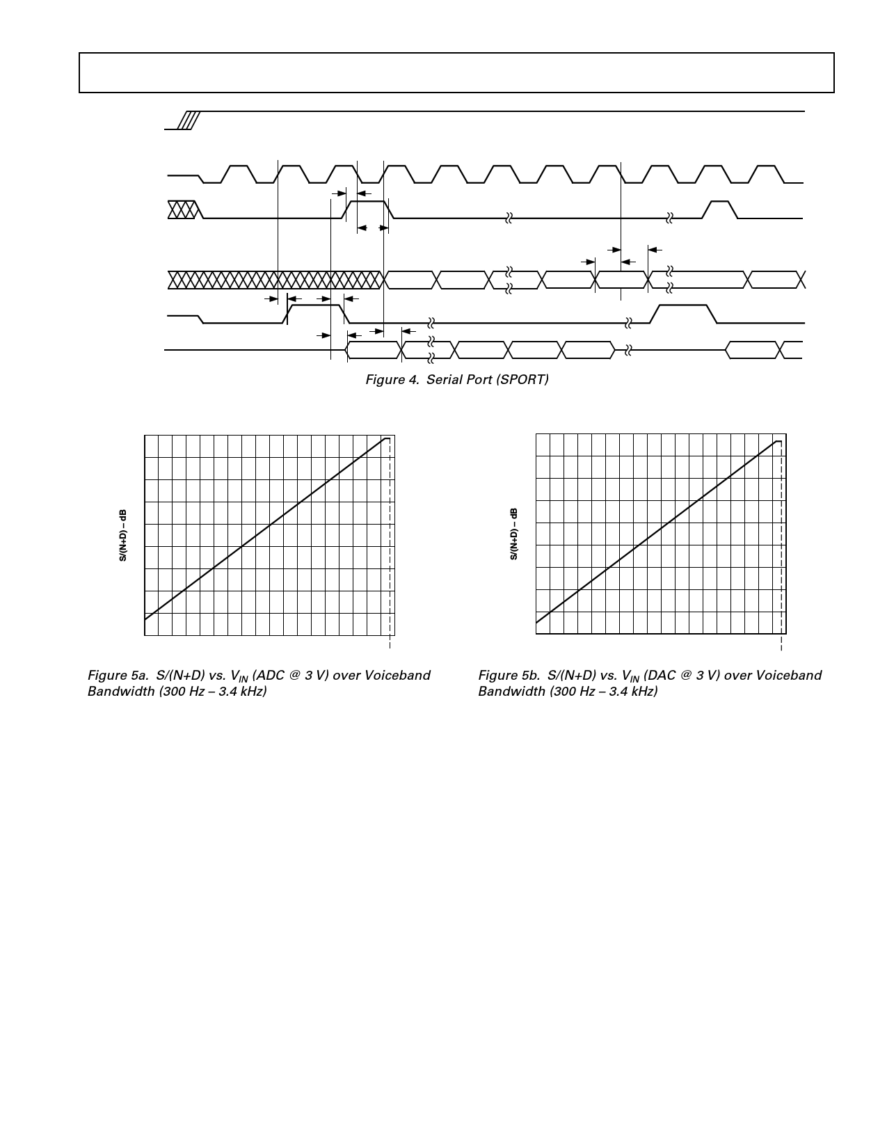
SE (I)
THREE-
SCLK (O) STATE
SDIFS (I)
SDI (I)
THREE-
SDOFS (O) STATE
THREE-
SDO (O) STATE
t9
t7
t8
D15
t10
D14
t8
t7
D1 D0
t12 t11
D15
D2 D1 D0
Figure 4. Serial Port (SPORT)
AD73311L
D15
D15 D14
80
70
60
50
40
30
20
10
0
–10
–85 –75 –65 –55 –45 –35 –25 –15 –5 0
VIN – dBm0
3.17
Figure 5a. S/(N+D) vs. VIN (ADC @ 3 V) over Voiceband
Bandwidth (300 Hz – 3.4 kHz)
80
70
60
50
40
30
20
10
0
–10
–85 –75 –65 –55 –45 –35 –25 –15 –5 0
VIN – dBm0
3.17
Figure 5b. S/(N+D) vs. VIN (DAC @ 3 V) over Voiceband
Bandwidth (300 Hz – 3.4 kHz)
REV. A
–5–
5 Page 
The output of the interpolation filter is fed to the DAC’s digital
sigma-delta modulator, which converts the 16-bit data to 1-bit
samples at a rate of DMCLK/8. The modulator noise-shapes
the signal so that errors inherent to the process are minimized
in the passband of the converter. The bitstream output of the
sigma-delta modulator is fed to the single bit DAC where it is
converted to an analog voltage.
Analog Smoothing Filter and PGA
The output of the single-bit DAC is sampled at DMCLK/8,
therefore it is necessary to filter the output to reconstruct the
low frequency signal. The decoder’s analog smoothing filter
consists of a continuous-time filter preceded by a third-order
switched-capacitor filter. The continuous-time filter forms part
of the output programmable gain amplifier (PGA). The PGA
can be used to adjust the output signal level from –15 dB to
+6 dB in 3 dB steps, as shown in Table IV. The PGA gain is
set by bits OGS0, OGS1 and OGS2 (CRD:4-6) in Control
Register D.
Table IV. PGA Settings for the Decoder Channel
OGS2
0
0
0
0
1
1
1
1
OGS1
0
0
1
1
0
0
1
1
OGS0
0
1
0
1
0
1
0
1
Gain (dB)
+6
+3
0
–3
–6
–9
–12
–15
Differential Output Amplifiers
The decoder has a differential analog output pair (VOUTP and
VOUTN). The output channel can be muted by setting the
MUTE bit (CRD:7) in Control Register D. The output signal
is dc-biased to the codec’s on-chip voltage reference.
Voltage Reference
The AD73311L reference, REFCAP, is a bandgap reference
that provides a low noise, temperature-compensated reference
to the DAC and ADC. A buffered version of the reference is
also made available on the REFOUT pin and can be used to
bias other external analog circuitry. The reference has a default
nominal value of 1.2 V.
The reference output (REFOUT) can be enabled for biasing
external circuitry by setting the RU bit (CRC:6) of CRC.
Serial Port (SPORT)
The codec communicates with a host processor via the bidirec-
tional synchronous serial port (SPORT) which is compatible
with most modern DSPs. The SPORT is used to transmit and
receive digital data and control information.
In both transmit and receive modes, data is transferred at the
serial clock (SCLK) rate with the MSB being transferred first.
Due to the fact that the SPORT uses a common serial register for
serial input and output, communications between an AD73311L
codec and a host processor (DSP engine) must always be initi-
ated by the codec itself. This ensures that there is no danger of
the information being sent to the codec being corrupted by
ADC samples being output by the codec.
AD73311L
SPORT Overview
The AD73311L SPORT is a flexible, full-duplex, synchronous
serial port whose protocol has been designed to allow up to eight
AD73311L devices to be connected, in cascade, to a single DSP
via a six-wire interface. It has a very flexible architecture that can
be configured by programming two of the internal control regis-
ters. The AD73311L SPORT has three distinct modes of opera-
tion: Control Mode, Data Mode and Mixed Control/Data Mode.
In Control Mode (CRA:0 = 0), the device’s internal configura-
tion can be programmed by writing to the five internal control
registers. In this mode, control information can be written to or
read from the codec. In Data Mode (CRA:0 = 1), information
that is sent to the device is used to update the decoder section
(DAC), while the encoder section (ADC) data is read from the
device. In this mode, only DAC and ADC data is written to or
read from the device. Mixed mode (CRA:0 = 1 and CRA:1 = 1)
allows the user to choose whether the information being sent to
the device contains either control information or DAC data.
This is achieved by using the MSB of the 16-bit frame as a flag
bit. Mixed mode reduces the resolution to 15 bits with the MSB
being used to indicate whether the information in the 16-bit
frame is control information or DAC/ADC data.
The SPORT features a single 16-bit serial register that is used
for both input and output data transfers. As the input and out-
put data must share the same register there are some precautions
that must be observed. The primary precaution is that no infor-
mation must be written to the SPORT without reference to an
output sample event, which is when the serial register will be
overwritten with the latest ADC sample word. Once the SPORT
starts to output the latest ADC word then it is safe for the DSP
to write new control or data words to the codec. In certain con-
figurations, data can be written to the device to coincide with
the output sample being shifted out of the serial register—see
section on interfacing devices. The serial clock rate (CRB:2–3)
defines how many 16-bit words can be written to a device before
the next output sample event will happen.
The SPORT block diagram, shown in Figure 9, details the six
control registers (A–F), external MCLK to internal DMCLK
divider and serial clock divider. The divider rates are controlled
by the setting of Control Register B. The AD73311L features a
master clock divider that allows users the flexibility of dividing
externally available high frequency DSP or CPU clocks to gener-
ate a lower frequency master clock internally in the codec which
may be more suitable for either serial transfer or sampling rate
requirements. The master clock divider has five divider options
(÷ 1 default condition, ÷ 2, ÷ 3, ÷ 4, ÷ 5) that are set by loading
the master clock divider field in Register B with the appropriate
code. Once the internal device master clock (DMCLK) has
been set using the master clock divider, the sample rate and
serial clock settings are derived from DMCLK.
The SPORT can work at four different serial clock (SCLK) rates:
chosen from DMCLK, DMCLK/2, DMCLK/4 or DMCLK/8,
where DMCLK is the internal or device master clock resulting
from the external or pin master clock being divided by the
master clock divider. When working at the lower SCLK rate of
DMCLK/8, which is intended for interfacing with slower DSPs,
the SPORT will support a maximum of two devices in cascade
with the sample rate of DMCLK/256.
REV. A
–11–
11 Page | ||
| Páginas | Total 30 Páginas | |
| PDF Descargar | [ Datasheet AD73311L.PDF ] | |
Hoja de datos destacado
| Número de pieza | Descripción | Fabricantes |
| AD73311 | Low Cost/ Low Power CMOS General Purpose Analog Front End | Analog Devices |
| AD73311L | Low Cost/ Low Power CMOS General Purpose Analog Front End | Analog Devices |
| Número de pieza | Descripción | Fabricantes |
| SLA6805M | High Voltage 3 phase Motor Driver IC. |
Sanken |
| SDC1742 | 12- and 14-Bit Hybrid Synchro / Resolver-to-Digital Converters. |
Analog Devices |
|
DataSheet.es es una pagina web que funciona como un repositorio de manuales o hoja de datos de muchos de los productos más populares, |
| DataSheet.es | 2020 | Privacy Policy | Contacto | Buscar |
