|
|
PDF ATF2500C-20JC Data sheet ( Hoja de datos )
| Número de pieza | ATF2500C-20JC | |
| Descripción | ATF2500C CPLD Family Datasheet | |
| Fabricantes | ATMEL Corporation | |
| Logotipo |  |
|
Hay una vista previa y un enlace de descarga de ATF2500C-20JC (archivo pdf) en la parte inferior de esta página. Total 30 Páginas | ||
|
No Preview Available !
.comFeatures
U• High-performance, High-density, Electrically-erasable Programmable Logic Device
t4• Fully Connected Logic Array with 416 Product Terms
e• 10 ns Maximum Pin-to-pin Delay for 5V Operation
e• Low-power Edge-sensing “L” Option with <1 mA Standby Current
h• 24 Flexible Output Macrocells
S– 48 Flip-flops – Two per Macrocell
ta– 72 Sum Terms
a– All Flip-flops, I/O Pins Feed in Independently
• D- or T-type Flip-flops
.D• Product Term or Direct Input Pin Clocking
w ATF2500C• Registered or Combinatorial Internal Feedback
w• Backward Compatible with ATV2500B/BQL and ATV2500H/L Software
CPLD Family• Advanced Electrically-erasable Technology
w– Reprogrammable
Datasmheet– 100% Tested
• 44-lead Surface Mount Package
.AcToF2500CBlock Diagram
Sheet4U AAAPTTTreFFFl222im555000in000aCCCrQLQyLDescription
taThe ATF2500C is the highest-density PLD available in a 44-pin package. With its fully
connected logic array and flexible macrocell structure, high gate utilization is easily
aobtainable. The ATF2500C is a high-performance CMOS (electrically-erasable) pro-
grammable logic device (PLD) that utilizes Atmel’s proven electrically-erasable
.Dtechnology.
wPin Configurations
Pin Name
wIN
w mCLK/IN
.coI/O
UI/O 0,2,4...
t4I/O 1,3,5...
eeGND
hVCC
Function
Logic Inputs
Pin Clock and Input
Bi-directional Buffers
“Even” I/O Buffers
“Odd” I/O Buffers
Ground
+5V Supply
DIP
IN
IN
IN
I/O0
I/O1
I/O2
I/O3
I/O4
I/O5
VCC
I/O17
I/O16
I/O15
I/O14
I/O13
I/O12
IN
IN
IN
IN
1
2
3
4
5
6
7
8
9
10
11
12
13
14
15
16
17
18
19
20
40 IN
39 IN
38 IN
37 IN
36 I/O6
35 I/O7
34 I/O8
33 I/O9
32 I/O10
31 I/O11
30 GND
29 I/O23
28 I/O22
27 I/O21
26 I/O20
25 I/O19
24 I/O18
23 IN
22 IN
21 IN
PLCC/LCC/JLCC
I/O2
I/O3
I/O4
I/O5
VCC
VCC
I/O17
I/O16
I/O15
I/O14
I/O13
7
8
9
10
11
12
13
14
15
16
17
39 I/O7
38 I/O8
37 I/O9
36 I/O10
35 I/O11
34 GND
33 GND
32 I/O23
31 I/O22
30 I/O21
29 I/O20
www.DataSNote:
For ATF2500CQ and ATF2500CQL
(PLCC/LCC/JLCC packages) pin 4 and pin 26
GND connections are not required.
Rev. 0777G–12/01
1
1 page 
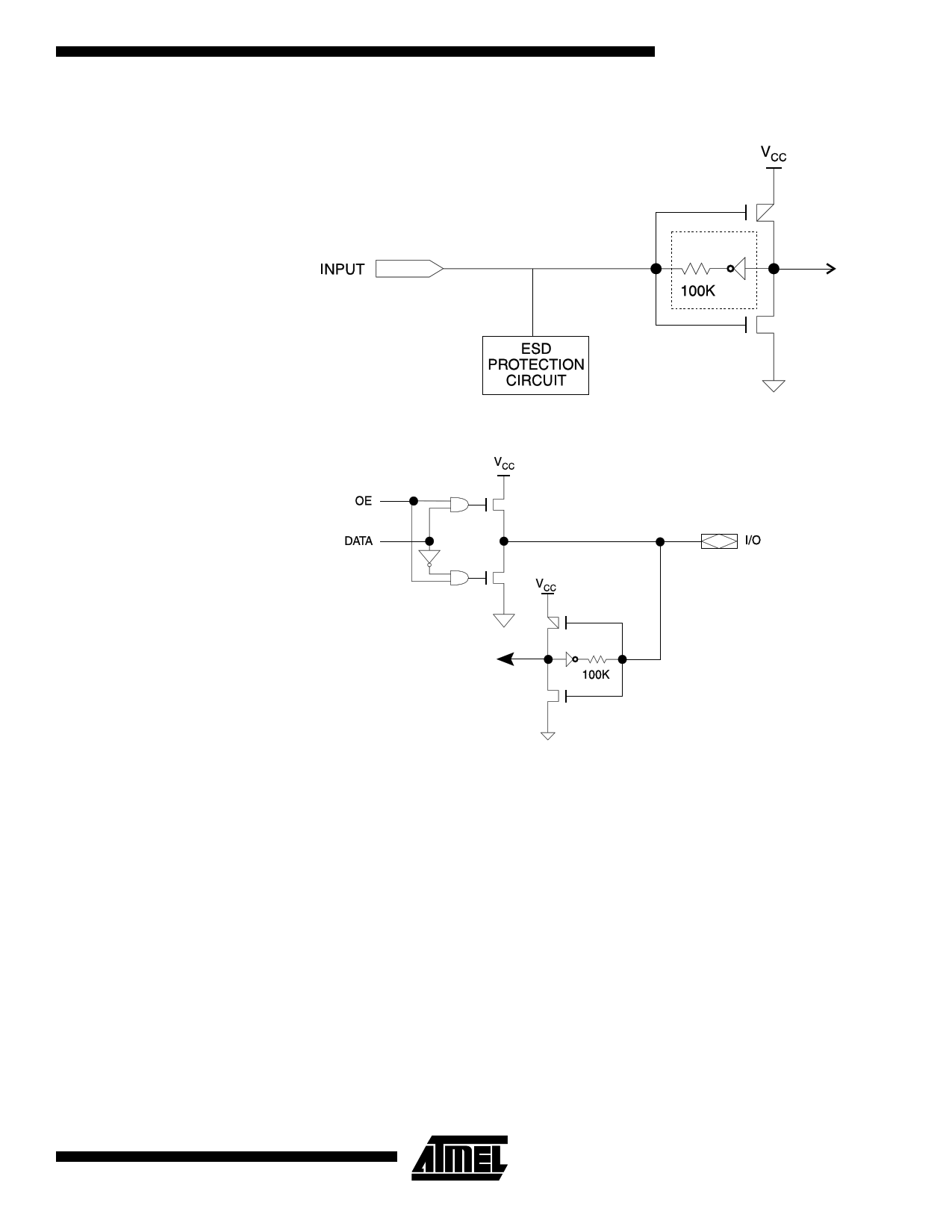
Input Diagram
ATF2500C Family
I/O Diagram
INPUT
Functional
Logic Diagram
Description
The ATF2500C functional logic diagram describes the interconnections between the input,
feedback pins and logic cells. All interconnections are routed through the single global bus.
The ATF2500Cs are straightforward and uniform PLDs. The 24 macrocells are numbered 0
through 23. Each macrocell contains 17 AND gates. All AND gates have 172 inputs. The five
lower product terms provide AR1, CK1, CK2, AR2, and OE. These are: one asynchronous
reset and clock per flip-flop, and an output enable. The top 12 product terms are grouped into
three sum terms, which are used as shown in the macrocell diagrams.
Eight synchronous preset terms are distributed in a 2/4 pattern. The first four macrocells share
Preset 0, the next two share Preset 1, and so on, ending with the last two macrocells sharing
Preset 7.
The 14 dedicated inputs and their complements use the numbered positions in the global bus
as shown. Each macrocell provides six inputs to the global bus: (left to right) feedback F2(1)
true and false, flip-flop Q1 true and false, and the pin true and false. The positions occupied by
these signals in the global bus are the six numbers in the bus diagram next to each macrocell.
Note: 1. Either the flip-flop input (D/T2) or output (Q2) may be fed back in the ATF2500Cs.
0777G–12/01
5
5 Page 
ATF2500C
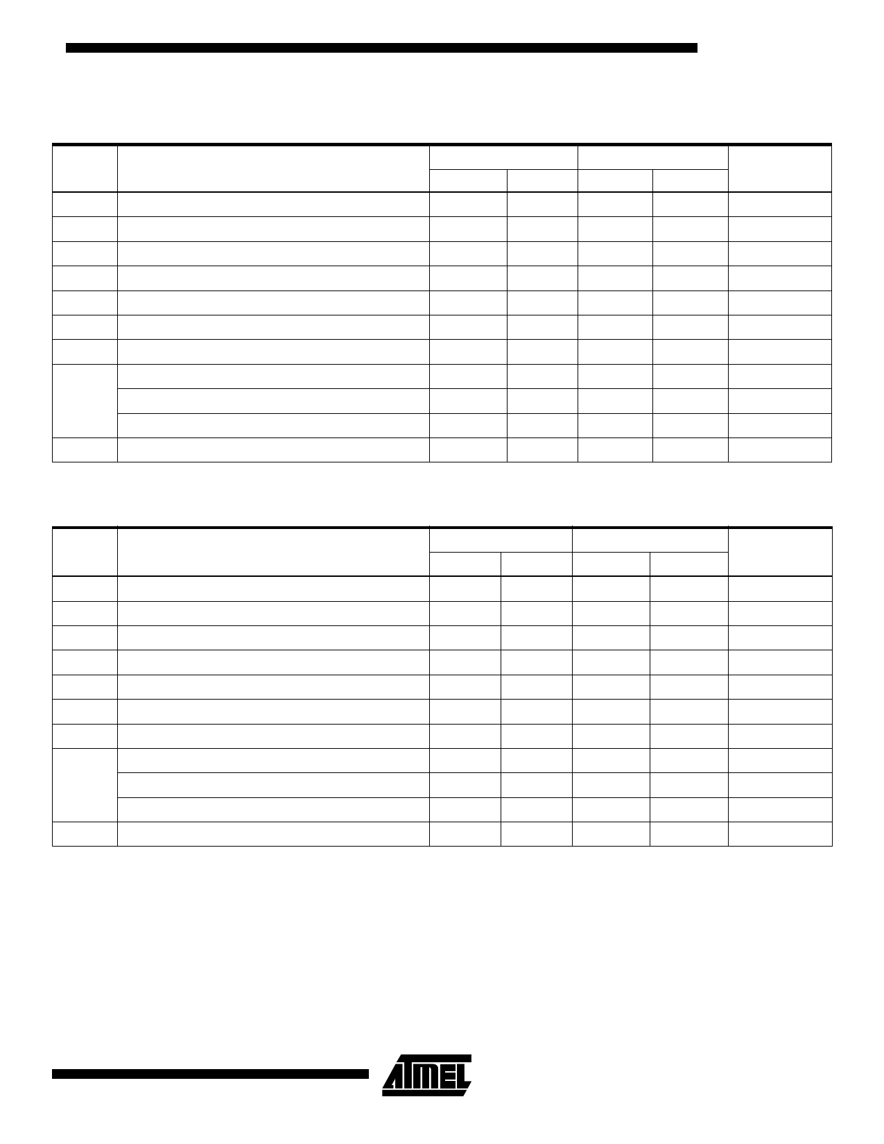
ATF2500C Register AC Characteristics, Input Pin Clock
Symbol
tCOS
tCFS
tSIS
tSFS
tHS
tWS
tPS
FMAXS
tARS
Parameter
Clock to Output
Clock to Feedback
Input Setup Time
Feedback Setup Time
Hold Time
Clock Width
Clock Period
External Feedback 1/(tSIS + tCOS)
Internal Feedback 1/(tSFS + tCFS)
No Feedback 1/(tPS)
Asynchronous Reset/Preset Recovery Time
-10
Min
0
2
2
0
3
8
5
Max
5.5
2
75
100
110
-15
Min
0
9
9
0
6
12
12
Max
10
5
52
71
83
ATF2500C Register AC Characteristics, Product Term Clock
Symbol
tCOA
tCFA
tSIA
tSFA
tHA
tWA
tPA
FMAXA
tARA
Parameter
Clock to Output
Clock to Feedback
Input Setup Time
Feedback Setup Time
Hold Time
Clock Width
Clock Period
External Feedback 1/(tSIA + tCOA)
Internal Feedback 1/(tSFA + tCFA)
No Feedback 1/(tPS)
Asynchronous Reset/Preset Recovery Time
-10
Min Max
10
25
2
2
1
3
9
75.5
100
100
2
-15
Min Max
15
5 12
5
5
5
7.5
15
50
58
66
8
Units
ns
ns
ns
ns
ns
ns
ns
MHz
MHz
MHz
ns
Units
ns
ns
ns
ns
ns
ns
ns
MHz
MHz
MHz
ns
0777G–12/01
11
11 Page | ||
| Páginas | Total 30 Páginas | |
| PDF Descargar | [ Datasheet ATF2500C-20JC.PDF ] | |
Hoja de datos destacado
| Número de pieza | Descripción | Fabricantes |
| ATF2500C-20JC | ATF2500C CPLD Family Datasheet | ATMEL Corporation |
| ATF2500C-20JI | ATF2500C CPLD Family Datasheet | ATMEL Corporation |
| Número de pieza | Descripción | Fabricantes |
| SLA6805M | High Voltage 3 phase Motor Driver IC. |
Sanken |
| SDC1742 | 12- and 14-Bit Hybrid Synchro / Resolver-to-Digital Converters. |
Analog Devices |
|
DataSheet.es es una pagina web que funciona como un repositorio de manuales o hoja de datos de muchos de los productos más populares, |
| DataSheet.es | 2020 | Privacy Policy | Contacto | Buscar |
