|
|
|
PDF 6817 Data sheet ( Hoja de datos )
| Número de pieza | 6817 | |
| Descripción | ADDRESSABLE 28-LINE DECODER/DRIVER | |
| Fabricantes | Allegro MicroSystems | |
| Logotipo | ||
Hay una vista previa y un enlace de descarga de 6817 (archivo pdf) en la parte inferior de esta página. Total 8 Páginas | ||
|
No Preview Available !
6817
ADDRESSABLE
28-LINE
DECODER/DRIVER
OUTB1 7
OUTB2 8
OUTB3 9
OUTB4 10
OUTB5 11
OUTB6 12
OUTB7 13
OUTB8 14
OUTB9 15
GND 16
IC 17
6817
39 OUTA0
38 OUTA1
37 OUTA2
36 OUTA3
35 OUTA4
34 OUTA5
33 OUTA6
32 OUTA7
31 OUTA8
30 OUTA9
29 GND
Dwg. PP-050
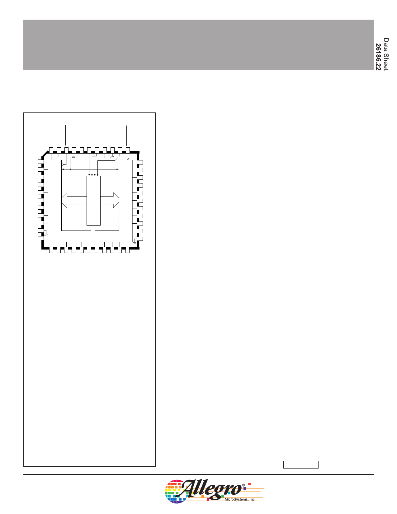
ADDRESSABLE
28-LINE DECODER/DRIVER
Intended for use in ink-jet printer applications, the A6817SEP
addressable 28-line decoder/driver combines low-power CMOS inputs
and logic with 28 high-current, high-voltage bipolar outputs. A 4-to-14
line decoder determines the selected output driver (n) in each
14-driver bank. Two independent output-enable inputs (active low)
then provide the final decoding to activate 1- or 2-of-28 outputs
(OUTAn and/or OUTBn). Special internal circuitry is programmed at the
time of manufacture to adjust the output pulse timing and thereby the
energy the device delivers to the ink-jet print head. The DABiC-IV
A6817SEP directly replaces the original BiMOS-II A5817SEP in most
applications.
The CMOS inputs cause minimal loading and are compatible with
standard CMOS, PMOS, and NMOS logic. Use with TTL or DTL
circuits may require appropriate pull-up resistors to ensure an input
logic high. The internal CMOS logic operates from a 5 V supply.
A CHIP ENABLE function is provided to lock out the drivers during
system power up. The 28 bipolar power outputs are open-collector
30 V Darlington drivers capable of sinking 500 mA at ambient
temperatures up to 85°C.
The A6817SEP is furnished in a 44-lead plastic chip carrier
(quad pack) for minimum-area, surface-mount applications.
ABSOLUTE MAXIMUM RATINGS
at TA = 25°C
Output Voltage, VCE ............................. 30 V
Logic Supply Voltage, VDD .................. 7.0 V
Input Voltage Range,
VIN ....................... -0.3 V to VDD + 0.3 V
Output Current, IC ........................... 600 mA
Package Power Dissipation, PD ..... 2.70 W*
Operating Temperature Range,
TA ................................. -20°C to +85°C
Storage Temperature Range,
TS .............................. -55°C to +150°C
*Derate at rate of 22 mW/°C above TA = 25°C.
Caution: These CMOS devices have input static
protection (Class 2) but are still susceptible to
damage when exposed to extremely high static
electrical charges.
FEATURES
s Controlled Characteristics for Ink-Jet Printers
s Addressable Data Entry
s 30 V Minimum V(BR)CEX
s CMOS, PMOS, NMOS Compatible Inputs
s Low-Power CMOS Logic
Always order by complete part number: A6817SEP .
1 page 
6817
ADDRESSABLE
28-LINE
DECODER/DRIVER
APPLICATIONS INFORMATION
This device is intended specifically for, although
certainly not limited to, driving ink-jet print heads. In
this application, a certain minimum energy (a function
of load voltage and output pulse duration) is required
for proper operation, while excessive energy will
degrade the life of the print head. The output pulse
duration (tOUT) is equal to tENABLE + tPLH – tPHL, where
tPHL is adjusted during manufacture to compensate for
variations in the output saturation voltage (VCE(SAT)).
For the A6817SEP, the relationship between tOUT
and tENABLE at TA = 25°C is:
tOUT = tENABLE ([VCE(SAT)(actual) – VCE(SAT)(typical)]
x 330 ns) + 25 ns + 110 ns.
For most applications, this will result in a driver-
contribution-to-energy-error of less than ±4%.
A logic low on the CHIP ENABLE input will
prevent the drivers from turning ON, regardless of the
state of other inputs or the logic supply voltage. The
CHIP ENABLE input has a slow response time and
should not be used as a high-speed control line. For
proper operation, all ground terminals should be
connected to a common ground on the printed wiring
board. The IC (Internal Connection) terminals are
used to program the turn-on time of the device and
MUST be left electrically unconnected (floating) for
proper operation.
IND
(MSB)
0
0
0
0
0
0
0
0
1
1
1
1
1
1
1
1
DECODER TRUTH TABLE
INC INB INA
(LSB)
N
0000
0011
0102
0113
1004
1015
1106
1117
0008
0019
0 1 0 10
0 1 1 11
1 0 0 12
1 0 1 13
1 1 0 ALL OFF
1 1 1 ALL OFF
Depending on the four address inputs, the 4-to-14 line
decoder selects one driver from each of the 14 output A
and B banks of sink drivers according to the Decoder
Truth Table. The state of the selected outputs is deter-
mined by the OUTPUT ENABLE inputs as shown in the
Enable Truth Table.
CHIP
ENABLE
0
1
1
1
1
X = Irrelevant
OUTPUT
ENABLEA
X
1
0
1
0
ENABLE TRUTH TABLE
OUTPUT
ENABLEB
X
1
1
0
0
OUTPUTS (OFF unless otherwise specified.
For the value of N see the Decoder Truth Table)
ALL OFF
ALL OFF
OUTAN ON
OUTBN ON
OUTAN ON, OUTBN ON
5 Page | ||
| Páginas | Total 8 Páginas | |
| PDF Descargar | [ Datasheet 6817.PDF ] | |
Hoja de datos destacado
| Número de pieza | Descripción | Fabricantes |
| 681 | RECTIFIERS ASSEMBLIES | Microsemi Corporation |
| 681-1 | RECTIFIERS ASSEMBLIES | Microsemi Corporation |
| 681-2 | RECTIFIERS ASSEMBLIES | Microsemi Corporation |
| 681-3 | RECTIFIERS ASSEMBLIES | Microsemi Corporation |
| Número de pieza | Descripción | Fabricantes |
| SLA6805M | High Voltage 3 phase Motor Driver IC. |
Sanken |
| SDC1742 | 12- and 14-Bit Hybrid Synchro / Resolver-to-Digital Converters. |
Analog Devices |
|
DataSheet.es es una pagina web que funciona como un repositorio de manuales o hoja de datos de muchos de los productos más populares, |
| DataSheet.es | 2020 | Privacy Policy | Contacto | Buscar |