|
|
|
PDF X40620 Data sheet ( Hoja de datos )
| Número de pieza | X40620 | |
| Descripción | Dual Voltage CPU Supervisor with 64K Serial EEPROM | |
| Fabricantes | Xicor | |
| Logotipo | ||
Hay una vista previa y un enlace de descarga de X40620 (archivo pdf) en la parte inferior de esta página. Total 17 Páginas | ||
|
No Preview Available !
64K X40620
Dual Voltage CPU Supervisor with 64K Serial EEPROM
FEATURES
• Dual Voltage Detection and Reset Assertion
—Three standard reset threshold settings. (3.1V/
2.6V, 3.1V/1.7V, 2.9V/2.3V)
—Adjust low voltage reset threshold voltages
using special programming sequence
—RESET signal valid down to VCC=1V
• Watchdog Timer (150ms)
• Power On Reset (150ms)
• Low Power CMOS
—10µA typical standby current, watchdog on
—400µA typical standby current, watchdog off
• 64kbit 2-Wire Serial EEPROM
—1MHz serial interface speed
—64-byte page write mode
—Self-timed write cycle
—5ms write cycle time (typical)
• 2.5 to 3.7V Power Supply Operation
• 8-Lead TSSOP package
DESCRIPTION
The X40620 combines several functions into one
device. The first is a dual voltage monitoring, power-on
reset control, watchdog timer and 64Kbit serial
EEPROM memory in one package. This combination
lowers system cost, reduces board space require-
ments, and increases reliability.
Applying voltage to VCC activates the power on reset
circuit which holds RESET active for a period of time.
This allows the power supply and system oscillator to
stabilize before the processor can execute code.
Low VCC detection circuitry protects the user’s system
from low voltage conditions, resetting the system when
VCC falls below the set minimum Vtrip point. RESET is
active until VCC returns to proper operating level and
stabilizes.
A second voltage monitor circuit (V2MON) tracks the
unregulated supply to provide a power fail warning or
monitors different power supply voltage. When the
second monitored voltage drops below a preset
V2TRIP voltage. V2FAIL is active until V2 returns to
proper operating level and above the V2TRIP voltage.
Five common low voltage combinations are available,
however, Xicor’s unique circuits allows the threshold
for either voltage monitor to be reprogrammed to meet
special needs or to fine-tune the threshold for applica-
tions requiring higher precision.
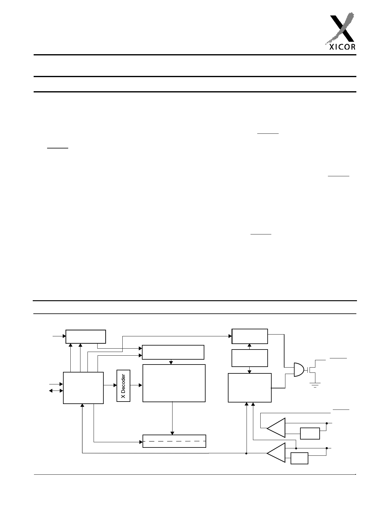
BLOCK DIAGRAM
WP
Write Control
Logic
SCL
SDA
Command
Decode
and
Control
Logic
HV Generation
Timing and Control
EEPROM Array
(64Kbits)
(VCC) Control Signal
Y Decoder
Data Register
Xicor, Inc. 2000 Patents Pending
9900-3003.5 4/24/00 EP
Watchdog
Timer Reset
Reset &
Watchdog
Timebase
Power on and
Low Voltage
Reset
Generation
RESET
+
- V2TRIP
+
- VTRIP
V2FAIL
V2MON
VCC
Characteristics subject to change without notice. 1 of 17
1 page 
X40620
Figure 5. Reset V2TRIP Level Sequence (VCC > 3V, WEL is set.)
VCC VTRIP
RESET
VP = 15V
0 1 23 4 56 7
01 23 4 56 7
01 23 4 56 7
01 23 4 56 7
SCL
SDA
D8h
00h 03h
03h resets VCC
00h
VCC AND V2MON THRESHOLD RESET PROCEDURE
The X40620 is shipped with standard VTRIP and
V2TRIP voltages. These values will not change over
normal operating and storage conditions. However, in
applications where the standard thresholds are not
exactly right, or if higher precision is needed in the
threshold value, the X40620 trip points may be
adjusted. The procedure is described below, and uses
the application of a high voltage control signal.
Setting the VTRIP Voltage
This procedure is used to set the VTRIP,V2TRIP to a
higher voltage value. For example, if the current VTRIP
is 4.4V and the new VTRIP is 4.6V, this procedure will
directly make the change. If the new setting is to be
lower than the current setting, then it is necessary to
reset the trip point before setting the new value.
To set the new voltages, apply the desired VTRIP thresh-
old voltage to the VCC pin, the V2TRIP voltage to the
V2MON pin, then tie the RESET pin to the programming
voltage VP. Then, write data 01h or 0Dh at address
00h to program VTRIP, V2TRIP respectively. The stop
bit following a valid write operation initiates the pro-
gramming sequence. Bring RESET LOW to complete
the operation. Note: this operation also writes 01h or
0Dh to address 00h.
Resetting the VTRIP Voltage
This procedure is used to set the VTRIP, the V2TRIP to
a “native” voltage level. For example, if the current
VTRIP is 4.4V and the new VTRIP must be 4.0V, then
the VTRIP must be reset. When the threshold is reset,
the new level is something less than 1.7V. This proce-
dure must be used to set the voltage to a lower value.
To reset the new VTRIP, V2TRIP voltage, apply the
desired VTRIP or V2TRIP threshold voltage to the
VCCor V2MON pin, respectively, and tie the RESET
pin to the programming voltage VP. Then write 03h or
0Fh to address 00h. The stop bit of a valid write opera-
tion initiates the programming sequence. Bring
RESET LOW to complete the operation. Note: this
operation also writes 03h or 0Fh to address 00h of the
EEPROM array.
Figure 6. Sample VTRIP Reset Circuit
VTRIP
Adj.
V2FAIL
RESET
V2TRIP
Adj.
4.7K
58
42
7 X40620 6
13
VP
Adjust
Run
µC
SCL
SDA
Characteristics subject to change without notice. 5 of 17
5 Page 
X40620
EQUIVALENT A.C. LOAD CIRCUIT
Output
3V
1.3KΩ
100pF
A.C. TEST CONDITIONS
Input pulse levels
Input rise and fall times
Input and output timing level
Output load
VCC x 0.1 to VCC x 0.9
10ns
VCC x 0.5
100pF
AC CHARACTERISTICS
AC Specifications (Over the recommended operating conditions)
Symbol
Parameter
fSCL
tIN
tAA
tBUF
tLOW
tHIGH
tSU:STA
tHD:STA
tSU:DAT
tHD:DAT
tSU:STO
tDH
tR
tF
SCL Clock Frequency
Pulse width of spikes which must be suppressed by the input filter
SCL LOW to SDA Data Out Valid
Time the bus must be free before a new transmit can start
Clock LOW Time
Clock HIGH Time
Start Condition Setup Time
Start Condition Hold Time
Data In Setup Time
Data In Hold Time
Stop Condition Setup Time
Data Output Hold Time
SDA and SCL Rise Time (10% to 90% of VCC)
SDA and SCL Fall Time
Min.
0
10
0.05
0.5
0.6
0.4
0.25
0.25
100
0
0.25
0
10
10
Typ.(1)
100
Max.
1000
0.55
100
100
Units
KHz
ns
µs
µs
µs
µs
µs
µs
ns
µs
µs
ns
ns
ns
RESET AC SPECIFICATIONS
Nonvolatile Write Cycle Timing
Symbol
tWC(1)
Parameter
Write Cycle Time
Min.
Typ.(1)
5
Max.
10
Units
mS
Notes: (1) tWC is the time from a valid stop condition at the end of a write sequence to the end of the self-timed internal nonvolatile write cycle.
It is the minimum cycle time to be allowed for any nonvolatile write by the user, unless Acknowledge Polling is used.
Characteristics subject to change without notice. 11 of 17
11 Page | ||
| Páginas | Total 17 Páginas | |
| PDF Descargar | [ Datasheet X40620.PDF ] | |
Hoja de datos destacado
| Número de pieza | Descripción | Fabricantes |
| X40620 | Dual Voltage CPU Supervisor with 64K Serial EEPROM | Xicor |
| X40626 | Dual Voltage CPU Supervisor with 64K Serial EEPROM | Xicor |
| X40626S14 | Dual Voltage CPU Supervisor with 64K Serial EEPROM | Xicor |
| X40626S14-2.7 | Dual Voltage CPU Supervisor with 64K Serial EEPROM | Xicor |
| Número de pieza | Descripción | Fabricantes |
| SLA6805M | High Voltage 3 phase Motor Driver IC. |
Sanken |
| SDC1742 | 12- and 14-Bit Hybrid Synchro / Resolver-to-Digital Converters. |
Analog Devices |
|
DataSheet.es es una pagina web que funciona como un repositorio de manuales o hoja de datos de muchos de los productos más populares, |
| DataSheet.es | 2020 | Privacy Policy | Contacto | Buscar |