|
|
|
PDF SMP04ES Data sheet ( Hoja de datos )
| Número de pieza | SMP04ES | |
| Descripción | CMOS Quad Sample-and-Hold Amplifier | |
| Fabricantes | Analog Devices | |
| Logotipo | ||
Hay una vista previa y un enlace de descarga de SMP04ES (archivo pdf) en la parte inferior de esta página. Total 15 Páginas | ||
|
No Preview Available !
a
FEATURES
Four Independent Sample-and-Holds
Internal Hold Capacitors
High Accuracy: 12 Bit
Very Low Droop Rate: 2 mV/s typ
Output Buffers Stable for CL ≤ 500 pF
TTL/CMOS Compatible Logic Inputs
Single or Dual Supply Applications
Monolithic Low Power CMOS Design
APPLICATIONS
Signal Processing Systems
Multichannel Data Acquisition Systems
Automatic Test Equipment
Medical and Analytical Instrumentation
Event Analysis
DAC Deglitching
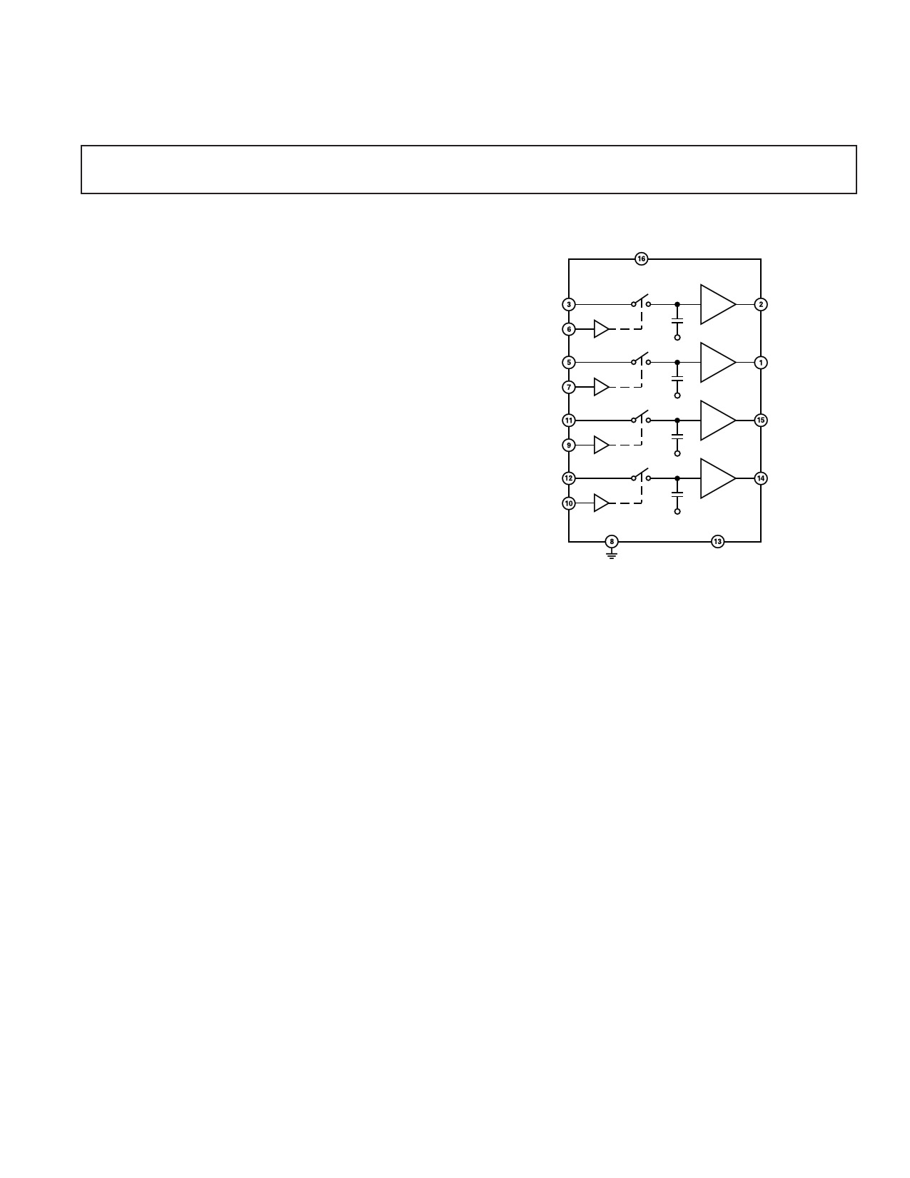
CMOS Quad
Sample-and-Hold Amplifier
SMP04*
FUNCTIONAL BLOCK DIAGRAM
VDD
SMP04
VIN1
S/H1
VIN2
S/H2
VIN3
S/H3
VIN4
S/H4
VSS
VSS
VSS
VSS
VOUT1
VOUT2
VOUT3
VOUT4
DGND
VSS
GENERAL DESCRIPTION
The SMP04 is a monolithic quad sample-and-hold; it has four
internal precision buffer amplifiers and internal hold capacitors.
It is manufactured in ADI’s advanced oxide isolated CMOS
technology to obtain the high accuracy, low droop rate and fast
acquisition time required by data acquisition and signal process-
ing systems. The device can acquire an 8-bit input signal to
± 1/2 LSB in less than four microseconds. The SMP04 can
operate from single or dual power supplies with TTL/CMOS
logic compatibility. Its output swing includes the negative supply.
The SMP04 is ideally suited for a wide variety of sample-and-
hold applications, including amplifier offset or VCA gain adjust-
ments. One or more can be used with single or multiple DACs
to provide multiple setpoints within a system.
The SMP04 offers significant cost and size reduction over
equivalent module or discrete designs. It is available in a
16-lead hermetic or plastic DIP and surface mount SOIC
packages. It is specified over the extended industrial tem-
perature range of –40°C to +85°C.
*Protected by U.S. Patent No. 4,739,281.
REV. D
Information furnished by Analog Devices is believed to be accurate and
reliable. However, no responsibility is assumed by Analog Devices for its
use, nor for any infringements of patents or other rights of third parties
which may result from its use. No license is granted by implication or
otherwise under any patent or patent rights of Analog Devices.
One Technology Way, P.O. Box 9106, Norwood, MA 02062-9106, U.S.A.
Tel: 781/329-4700
World Wide Web Site: http://www.analog.com
Fax: 781/326-8703
© Analog Devices, Inc., 1998
1 page 
10000
1000
VDD = +12V
VSS = 0V
VIN = +5V
RL = 10k⍀
100
10
0
–55 –35 –15 5 25 45 65 85 105 125
TEMPERATURE – ؇C
Figure 1. Droop Rate vs. Temperature
Typical Performance Characteristics–SMP04
5
VDD = +12V
VSS = 0V
3
1
0
–1
–3
–5
0 1 2 3 4 5 6 7 8 9 10
INPUT VOLTAGE – Volts
Figure 2. Droop Rate vs. Input
Voltage (TA = +25°C)
1800
1600
VDD = +12V
VSS = 0V
1400
1200
1000
800
600
0 1 2 3 4 5 6 7 8 9 10
INPUT VOLTAGE – Volts
Figure 3. Droop Rate vs. Input
Voltage (TA = +125°C)
3
TA = +25؇C
2
VDD = +12V
VSS = 0V
1
0
–1
–2
–3
01
23 456 78
INPUT VOLTAGE – Volts
9 10
Figure 4. Hold Step vs. Input Voltage
3
VDD = +12V
VSS = 0V
2 VIN = +5V
1
0
–1
–2
–3
–55 –35 –15 5 25 45 65 85 105 125
TEMPERATURE – ؇C
Figure 5. Hold Step vs. Temperature
7
TA = +25؇C
VSS = 0V
6
–SR
5
+SR
4
3
10 11 12 13 14 15 16 17 18
VDD – Volts
Figure 6. Slew Rate vs. VDD
2
VDD = +12V
VSS = 0V
1
0 RL =
–1 RL = 20k⍀
–2
RL = 10k⍀
–3
–4
0 1 2 3 4 5 6 7 8 9 10
INPUT VOLTAGE – Volts
Figure 7. Offset Voltage vs. Input
Voltage (TA = +25°C)
20
VDD = +12V
15 VSS = 0V
10
5 RL =
RL = 20k⍀
0
–5
–10
RL = 10k⍀
–15
–20
0 1 2 3 4 5 6 7 8 9 10
INPUT VOLTAGE – Volts
Figure 8. Offset Voltage vs. Input
Voltage (TA = +125°C)
4
VDD = +12V
2 VSS = 0V
RL =
0
RL = 20k⍀
–2
–4
–6 RL = 10k⍀
–8
–10
01
23456 78
INPUT VOLTAGE – Volts
9 10
Figure 9. Offset Voltage vs. Input
Voltage (TA = –55°C)
REV. D
–5–
5 Page 
VIN
(؎3.5V)
RESET
PD/H
POSITIVE
PD/H
NEGATIVE
AMPLIFIER A
+5V
1/2 OP221
–5V
AMPLIFIER B
1/2 OP221
R1
20k⍀
D1
1N914
D2
G
SD214
R2
100⍀
D
S Q1
R3
20k⍀
D3
1N914
D4
G
SD214
R4
100⍀
D
S Q2
+5V
VDD
–5V
VSS
VSS
1/2 SMP04
VSS
DGND
Figure 21. Positive and Negative Peak Detector with Hold Control
SMP04
VOUT
POSITIVE
VOUT
NEGATIVE
POSITIVE AND NEGATIVE PEAK DETECTOR WITH
HOLD CONTROL (Figure 21)
In this application the top amplifier (Amplifier A) is the positive
peak detector and the bottom amplifier (Amplifier B) is the
negative peak detector. Operation can be analyzed as follows:
Assume that the S/H switch is closed. As a positive increasing
voltage is applied to VIN, D2 turns on, and D1 turns off, closing
the feedback loop around Amplifier A and the SMP04, causing
the output to track the input. Conversely, in the negative peak
detector circuit at the bottom, D4 turns off and D3 turns on,
holding the last most negative input voltage on the SMP04.
This voltage is buffered to the VO(NEG) output.
As VIN falls in voltage the above conditions reverse, causing the
most positive peak voltage to be held at VO(POS) output. This
voltage will be held until the input has a more positive voltage
than the previously held peak voltage, or a reset condition is
applied.
An optional HOLD control can be used by applying a logic HIGH
to the PD/H inputs. This HOLD mode further reduces leakage
current through the reverse-biased diodes (D2 and D4) during
peak hold.
GAIN OF 10 SAMPLE-AND-HOLD (Figure 22)
This application places the SMP04 in a feedback loop of an
amplifier. Because the SMP04 has no sign inversion and the
amplifier has very high open-loop gain, the gain of the circuit is set
by the ratio of the sum of the source and feedback resistances
1k⍀
VIN
0V TO
1.0V
8.66k⍀
+12V
340⍀
1N914
+12V
1/4 SMP04
1/4 OP490
100k⍀
VSS
VOUT
0V TO
10V
S/H
Figure 22. Gain of 10 Sample-and-Hold Amplifier
to the source resistance. When a logic LOW is applied to the
S/H control input, the loop is closed around the OP490,
yielding a gain of 10 (in the example shown) amplifier. When
the S/H control goes HIGH, the loop opens and the SMP04
holds the last sampled voltage. The loop remains open and the
output is unaffected by the input until a logic LOW is reapplied
to the S/H control. The pair of back-to-back diodes from the
output of the op amp to the output of the track-and-hold pre-
vents the op amp from saturating when the track-and-hold is in
the hold mode and the loop is open.
REV. D
–11–
11 Page | ||
| Páginas | Total 15 Páginas | |
| PDF Descargar | [ Datasheet SMP04ES.PDF ] | |
Hoja de datos destacado
| Número de pieza | Descripción | Fabricantes |
| SMP04EP | CMOS Quad Sample-and-Hold Amplifier | Analog Devices |
| SMP04EQ | CMOS Quad Sample-and-Hold Amplifier | Analog Devices |
| SMP04ES | CMOS Quad Sample-and-Hold Amplifier | Analog Devices |
| Número de pieza | Descripción | Fabricantes |
| SLA6805M | High Voltage 3 phase Motor Driver IC. |
Sanken |
| SDC1742 | 12- and 14-Bit Hybrid Synchro / Resolver-to-Digital Converters. |
Analog Devices |
|
DataSheet.es es una pagina web que funciona como un repositorio de manuales o hoja de datos de muchos de los productos más populares, |
| DataSheet.es | 2020 | Privacy Policy | Contacto | Buscar |