|
|
|
PDF W137 Data sheet ( Hoja de datos )
| Número de pieza | W137 | |
| Descripción | Bx Notebook System Frequency Synthesizer | |
| Fabricantes | Cypress Semiconductor | |
| Logotipo | ||
Hay una vista previa y un enlace de descarga de W137 (archivo pdf) en la parte inferior de esta página. Total 10 Páginas | ||
|
No Preview Available !
W137
Bx Notebook System Frequency Synthesizer
Features
• Maximized EMI suppression using Cypress’s Spread
Spectrum Technology
• Two copies of CPU output
• Six copies of PCI output (Synchronous w/CPU output)
• One 48-MHz output for USB support
• One selectable 24-/48-MHz output
• Two Buffered copies of 14.318-MHz input reference
signal
• Supports 100-MHz or 66-MHz CPU operation
• Power management control input pins
• Available in 28-pin SSOP (209 mils)
• SS function can be disabled
• See W40S11-02 for 2 SDRAM DIMM support
Key Specifications
Supply Voltages: ....................................... VDDQ3 = 3.3V±5%
VDDQ2 = 2.5V±5%
CPU0:1 Output to Output Skew: ................................ 175 ps
CPU0:1 Cycle to Cycle Jitter: ..................................... 200 ps
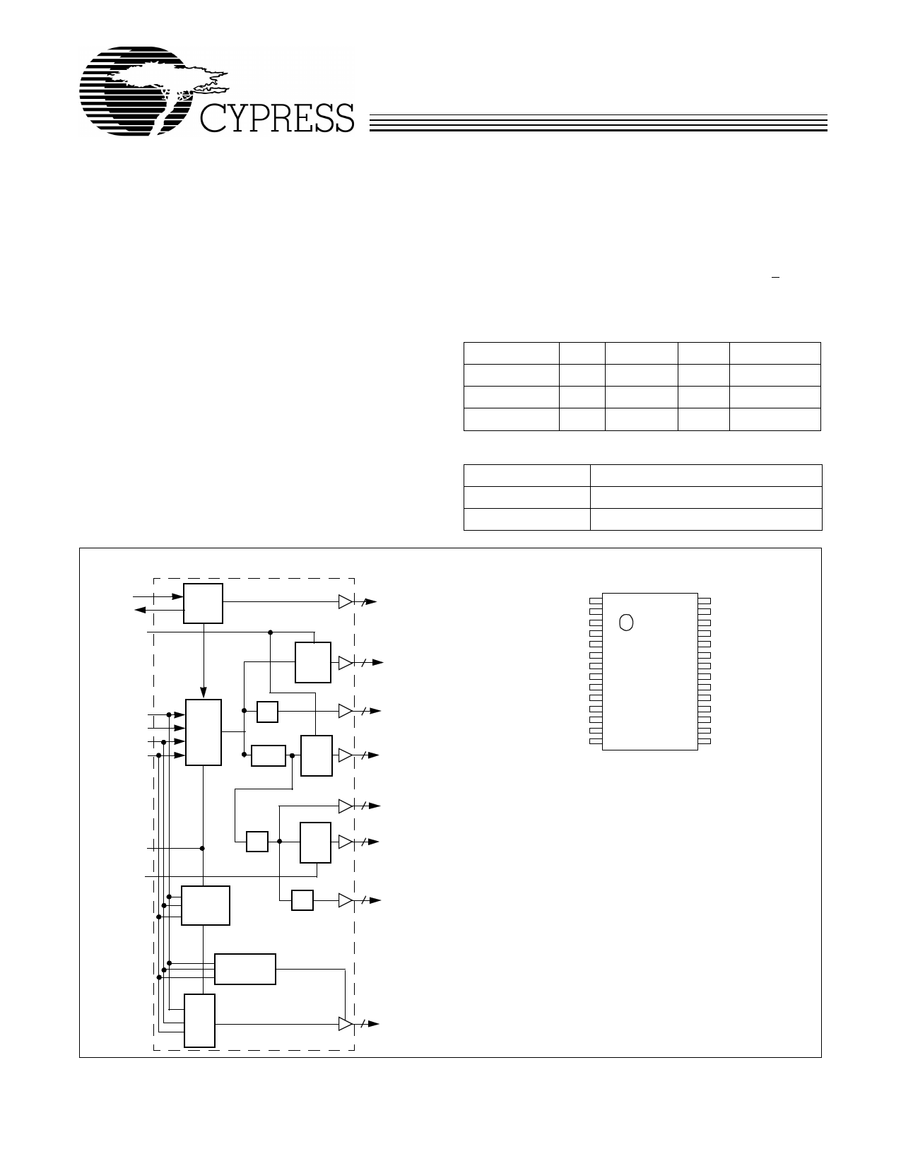
Block Diagram
PCI_F, PCI1:5 Output to Output Skew:........................ 500 ps
PCI_F, PCI1:5 Cycle to Cycle Jitter: ............................ 250 ps
CPU to PCI Output Skew: ............... 1.5–4.0 ns (CPU Leads)
Output Duty Cycle: .................................................... 45/55%
PCI_F, PCI Edge Rate: .............................................. >1 V/ns
CPU_STOP#, OE, SPREAD#, SEL48#, PCI_STOP#,
PWR_DWN# all have a 250-kΩ pull-up resistor.
Table 1. Pin Selectable Frequency
SEL100/66# OE
CPU
PCI Spread%
0/1
0
HI-Z
HI-Z Don’t Care
0 1 66.6 MHz 33.3 See Table 2
1 1 100 MHz 33.3 See Table 2
Table 2. Spread Spectrum Feature
SPREAD#
Spread Profile
0 –0.5% (down spread)
1 0% (spread disabled)
Pin Configuration
X1
X2
CPU_STOP#
SPREAD#
SEL0
SEL1
SEL133/100#
PWRDWN#
PCI_STOP#
XTAL
OSC
2
REF0:1
PLL 1
Power
Down
Logic
STOP
Clock
Logic
÷2
÷2/÷1.5
STOP
Clock
Logic
STOP
÷2 Clock
Logic
÷2
4
CPU0:3
2
CPUdiv2_0:1
4
3V66_0:3
1
PCI_F
7
PCI1:7
3
IOAPIC0:2
GND
X1
X2
PCI_F
PCI1
PCI2
GND
VDDQ3
PCI3
PCI4
PCI5
VDDQ3
48MHz
24/48MHz/OE
1
2
3
4
5
6
7
8
9
10
11
12
13
14
28 VDDQ3
27 REF0/SEL48#
26 REF1/SPREAD#
25 VDDQ2
24 CPU0
23 CPU1
22 GND
21 GND
20 PCI_STOP#
19 VDDQ3
18 CPU_STOP#
17 PWR_DWN#
16 SEL100/66#
15 GND
Three-state
Logic
PLL2
1
48MHz
Cypress Semiconductor Corporation • 3901 North First Street • San Jose • CA 95134 • 408-943-2600
October 12, 1999, rev. **
1 page 
W137
Absolute Maximum Ratings
Stresses greater than those listed in this table may cause per-
manent damage to the device. These represent a stress rating
only. Operation of the device at these or any other conditions
.
Parameter
Description
VDD, VIN
TSTG
TA
TB
ESDPROT
Voltage on any pin with respect to GND
Storage Temperature
Operating Temperature
Ambient Temperature under Bias
Input ESD Protection
above those specified in the operating sections of this specifi-
cation is not implied. Maximum conditions for extended peri-
ods may affect reliability.
Rating
–0.5 to +7.0
–65 to +150
0 to +70
–55 to +125
2 (min.)
Unit
V
°C
°C
°C
kV
DC Electrical Characteristics:
TA = 0°C to +70°C; VDDQ3 = 3.3V±5%; VDDQ2 = 2.5V±5%; CPU0:1 = 66.6/100 MHz
Parameter
Description
Test Condition
Min.
Typ.
Max. Unit
Supply Current
IDD3PD
3.3V Supply Current in Power-down mode
IDD3 3.3V Supply Current
IDD2 2.5V Supply Current
IDD2PD
2.5V Supply Current in Power-down mode
Logic Inputs
PWR_DWN# = 0
Outputs Loaded[1]
Outputs Loaded[1]
PWR_DWN# = 0
1 5 mA
80 100 mA
30 45 mA
0.2 µA 1 mA
VIL Input Low Voltage
VIH Input High Voltage
IIL Input Low Current[2]
IIH Input High Current[2]
IIL Input Low Current (SEL100/66#)
IIH Input High Current (SEL100/66#)
Clock Outputs
GND – 0.3
2.0
0.8
VDD + 0.3
–25
10
–5
+5
V
V
µA
µA
µA
µA
VOL Output Low Voltage
VOH Output High Voltage
PCI_F, PCI1:5,
REF0:1
IOL = 1 mA
IOH = –1 mA
3.1
50 mV
V
VOH Output High Voltage
CPU0:1
IOH = –1 mA
2.2
V
IOL Output Low Current: CPU0:1
VOL = 1.25V
80 120 180 mA
PCI_F, PCI1:5
VOL = 1.5V
70 110 140 mA
REF0:1
VOL = 1.5V
50 70 90 mA
IOH Output High Current
CPU0:1
VOH = 1.25V
80 120 180 mA
PCI_F, PCI1:5
VOH = 1.5V
70 110 140 mA
REF0:1
VOH = 1.5V
50 70 90 mA
Crystal Oscillator
VTH
CLOAD
CIN,X1
X1 Input Threshold Voltage[3]
Load Capacitance, As Seen by External Crystal[4]
X1 Input Capacitance[5]
VDDQ3 = 3.3V
Pin X2 unconnected
1.65
14
28
V
pF
pF
Notes:
1. All clock outputs loaded with 6" 60Ω transmission lines with 20-pF capacitors.
2. CPU_STOP#, PCI_STOP#, PWR_DWN#, SPREAD#, and SEL48# logic inputs have internal pull-up resistors (not CMOS level).
3. X1 input threshold voltage (typical) is VDD/2.
4. The W137 contains an internal crystal load capacitor between pin X1 and ground and another between pin X2 and ground. Total load placed on crystal is
14 pF; this includes typical stray capacitance of short PCB traces to crystal.
5. X1 input capacitance is applicable when driving X1 with an external clock source (X2 is left unconnected).
5
5 Page | ||
| Páginas | Total 10 Páginas | |
| PDF Descargar | [ Datasheet W137.PDF ] | |
Hoja de datos destacado
| Número de pieza | Descripción | Fabricantes |
| W130 | Spread Spectrum Desktop/Notebook System Clock | Cypress Semiconductor |
| W13009 | STW13009 | STMicroelectronics |
| W130L | Sensick | Sick |
| W132 | Spread Aware/ Ten/Eleven Output Zero Delay Buffer | Cypress Semiconductor |
| Número de pieza | Descripción | Fabricantes |
| SLA6805M | High Voltage 3 phase Motor Driver IC. |
Sanken |
| SDC1742 | 12- and 14-Bit Hybrid Synchro / Resolver-to-Digital Converters. |
Analog Devices |
|
DataSheet.es es una pagina web que funciona como un repositorio de manuales o hoja de datos de muchos de los productos más populares, |
| DataSheet.es | 2020 | Privacy Policy | Contacto | Buscar |