|
|
|
PDF WM8144 Data sheet ( Hoja de datos )
| Número de pieza | WM8144 | |
| Descripción | Integrated 10-bit Data Acquisition system for Imaging Applications | |
| Fabricantes | Wolfson Microelectronics plc | |
| Logotipo | ||
Hay una vista previa y un enlace de descarga de WM8144 (archivo pdf) en la parte inferior de esta página. Total 27 Páginas | ||
|
No Preview Available !
WM8144-10
Production Data
October 1997 Rev. 3.0
Integrated 10-bit Data Acquisition system for
Imaging Applications
Description
Features
WM8144-10 integrates the analogue signal conditioning
required by CCD sensors with a 10-bit ADC and optional
pixel-by-pixel image compensation. WM8144-10 requires
minimal external circuitry and provides a cost effective
sensor-to-digital domain system solution.
Each analogue conditioning channel provides reset level
clamp, CDS, fine offset level shifting and gain
amplification. The three channels are multiplexed into the
ADC. Output from the ADC can either be direct or passed
through a digital post-processing function. The post-
processing provides compensation for variations in offset
and shading on a pixel-by-pixel basis.
• Reset level clamp
• Correlated Double Sampling (CDS)
• Fine offset level shifting
• Programmable Gain Amplification
• 10-Bit ADC with maximum 6 MSPS
• Digital post-processing for pixel-by-pixel
image compensation
• Simple clocking scheme
• Control by serial or parallel interface
• Time-multiplexed eight-bit data output mode
• 48 pin TQFP package
• Pin compatible with WM8144-12
The flexible output architecture allows ten-bit data to be
accessed either on a ten-bit bus or via a time-multiplexed
eight-bit bus. The WM8144-10 can be configured for pixel-
by-pixel or line-by-line multiplexing operation. Reset level
clamp and/or CDS features can be optionally bypassed.
Device configuration is either by a simple serial or eight-
bit parallel interface.
Applications
• Document scanners
• CCD sensor interfaces
• Contact image sensor (CIS) interfaces
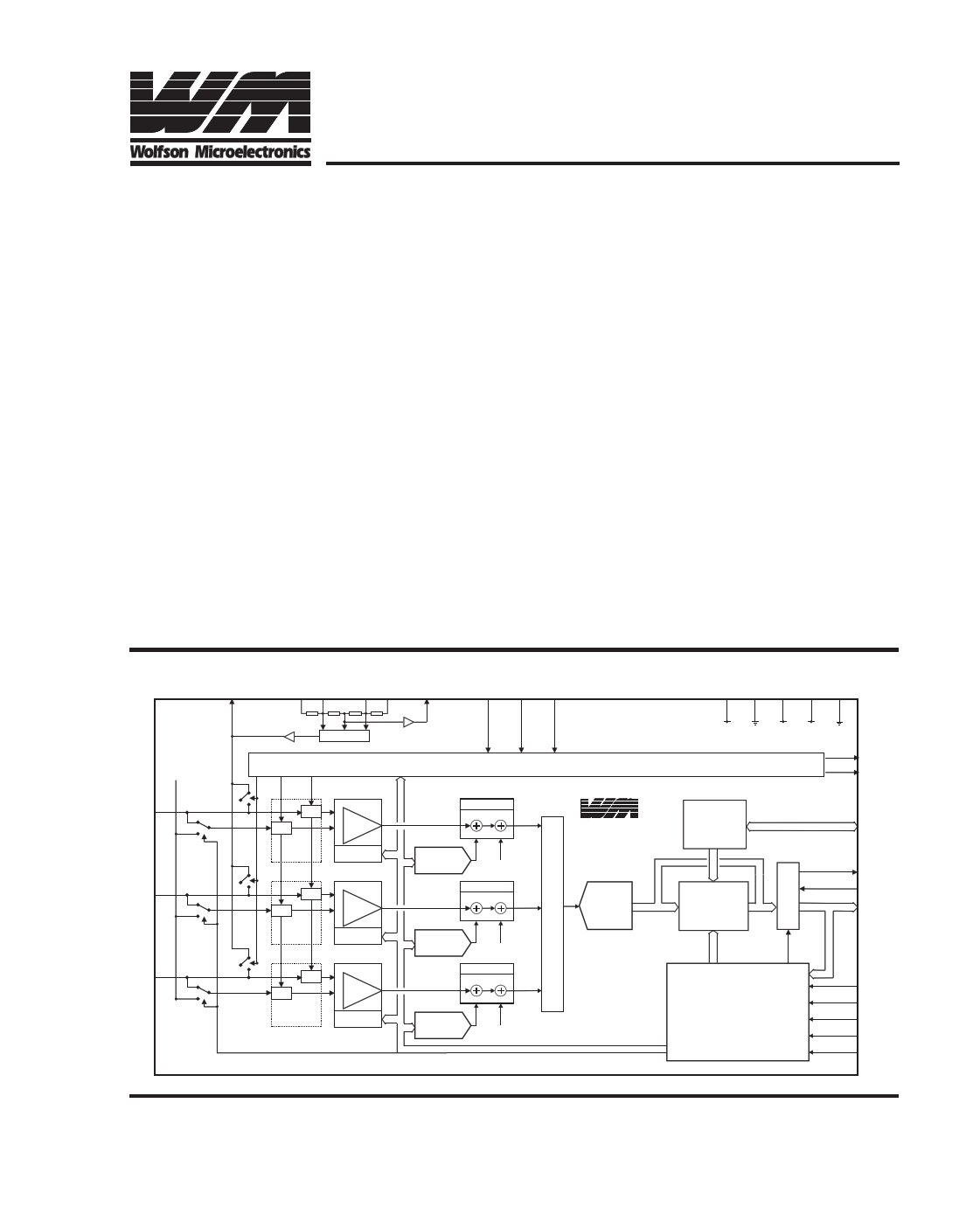
Block Diagram
VRLC
VRU VRT
VRB VRL
VMID
VSMP MCLK RLC
AVDD AGND DVDD1 DVDD2 DGND
VMID
RINP
GINP
BINP
MUX
CL RS VS
S/H
S/H
PGA
CDS
5-BIT REG
S/H
S/H
PGA
CDS
5-BIT REG
S/H
S/H
PGA
CDS
5-BIT REG
TIMING CONTROL
OFFSET
8-BIT + SIGN
DAC
VMID
OFFSET
8-BIT + SIGN
DAC
VMID
OFFSET
8-BIT + SIGN
DAC
VMID
WM8144-10
EXTERNAL
DATA STORE
INTERFACE
M
U
X
10 BIT
ADC
IMAGE
COMPENSATION
PROCESSING
10/8
MUX
CONFIGURABLE
SERIAL/PARALLEL
CONTROL INTERFACE
CC[2:0]
DV
CDATA(7:0)
ORNG
OEB
OP[9:0]
PNS
SDI / DNA
SCK / RNW
SEN / STB
NRESET
Production Data data sheets contain fi-
nal specifications current on publication
date. Supply of products conforms to
Wolfson Microelectronics standard terms
and conditions
Wolfson Microelectronics
Lutton Court, Bernard Terrace, Edinburgh EH8 9NX, UK
Tel: +44 (0) 131 667 9386 Fax: +44 (0) 131 667 5176
email: [email protected]
www: http://www.wolfson.co.uk
© 1997 Wolfson Microelectronics
1 page 
WM8144-10
Electrical Characteristics (Contd.)
VDD = 4.75V to 5.25V, GND = 0 V, ........TA = 0oC to +70oC, MLCK = 12MHz unless otherwise stated.
PARAMETER
Switching Characteristics
MCLK Period
MCLK High
MCLK Low
Data Set-up time
VSMP, RLC Data Hold Time
CDATA Data Hold Time
Output Propagation Delay
Output Enable TIme
Output Disable Time
Serial Interface
SCK Period
SCK High
SCK Low
SDI Set up time
SDI Hold Time
Set up time - SCK to SEN
Set up time - SEN to SCK
SEN Pulse W idth
Parallel Interface
RNW Low to OP[9:2] Tristate
Address Setup Time to STB Low
DNA Low Setup Time to STB Low
Strobe Low Time
Address Hold Time from STB High
DNA Low Hold Time from STB High
Data Set-up Time to STB Low
DNA High Setup Time to STB Low
Data Hold Time from STB High
DNA High Hold Time from STB High
RNW High to OP[9:2] Output
TEST CONDITIONS
tPER
tCKH
tCKL
tDSU
tDH
tDH
tPD IOH = 1.0mA
tPZE IOL = 1.0mA
tPEZ
tSPER
tSCKH
tSCKL
tSSU
tSH
tSCE
tSEC
tSEW
tOPZ
tASU
tADLS
tSTB
tAH
tADLH
tDSU
tADHS
tDH
tADHH
tOPD
MIN
83.3
37.5
37.5
10
10
30
83.3
37.5
37.5
10
10
20
20
50
0
10
50
10
10
0
10
10
10
0
TYP
MAX UNIT
ns
ns
ns
ns
ns
ns
75 ns
75 ns
25 ns
ns
ns
ns
ns
ns
ns
ns
ns
20 ns
ns
ns
ns
ns
ns
ns
ns
ns
ns
ns
Wolfson Microelectronics
5
5 Page 
WM8144-10
Theory of Operation (contd.)
The position of the clamp relative to the video sample is
programmable by CDSREF1-0 (see Table 7). By default,
the reset sample occurs on the fourth MCLK rising edge
after VSMP. The relative timing between the reset sam-
ple ( and CL) and video sample can be altered as shown
in Figure 4.
Video Input
Clamp Pulse
Figure 5
A reset level clamp is activated if the RLC pin is high on
an MCLK rising edge (Figure 6). By default this initiates
an internal clamp pulse three MCLK pulses later (Figure
4: CL). The relationship between CL and RS is fixed.
Therefore altering the RS position also alters the CL po-
sition (Figure 4). Table 7 shows the three possible voltages
to which the reset level can be clamped.
Figure 4: Reset Sample and Clamp Timing
When the clamp pulse is active the voltage on the
WM8144-10 side of Cin, i.e. RINP, will be forced to be
equal to the VRLC clamp voltage (see Figure 5). The
VRLC clamp voltage is programmable to three different
levels via the serial interface (1.5V, 2.5V or 3.5V). The
voltage to which the clamp voltage should be programmed
is dependent on the type of sampling selected and the
polarity of the input video signal. For CDS operation it is
important to match the clamp voltage to the amplitude
and polarity of the video signal. This will allow the best
use of the wide input common-mode range offered by the
WM8144-10. If the input video is positive going it is ad-
visable to clamp to Vcl (Lower clamp voltage). If the video
is negative going it is advisable to clamp to Vcu (Upper
clamp voltage). Regardless of where the video is clamped
the offset DAC is programmed to move the ADC output
corresponding to the reset level to an appropriate value
to maximise the ADC dynamic range. For Single Ended
operation it is recommended that the clamp voltage is set
to Vcm (Middle clamp voltage).
Figure 6: RLC Timing
RINP, GINP and BINP Input Impedence
The input impedence of the WM8144-10 analogue inputs
is dependent on the sampling frequency of the input sig-
nal and the configuration of the internal gain amplifiers.
The input impedence = 1/(Capacitance * frequency)
where the Capacitance value changes from 0.3pF for
minimum gain to 9.6pF for maximum gain. Table 1 illus-
trates the minimum and maximum input impedence at
different frequencies.
Sampling
Frequency
(MHz)
0.5
1
2
4
6
Impedence with
minimum gain
(MΩ)
6.6
3.3
1.6
0.8
0.5
Impedence with
maximum gain
(KΩ)
208
104
52
26
17
Table 1: Effects of Frequency on Input Impedence
Wolfson Microelectronics
11
11 Page | ||
| Páginas | Total 27 Páginas | |
| PDF Descargar | [ Datasheet WM8144.PDF ] | |
Hoja de datos destacado
| Número de pieza | Descripción | Fabricantes |
| WM8141 | 12-bit 6MSPS CIS/CCD Analogue Front End/Digitiser | Wolfson Microelectronics plc |
| WM8143-10 | 10-bit/6MSPS CCD Signal Processor | Wolfson Microelectronics plc |
| WM8143-12 | 12-bit/4MSPS CCD Signal Processor | Wolfson Microelectronics plc |
| WM8144 | Integrated 10-bit Data Acquisition system for Imaging Applications | Wolfson Microelectronics plc |
| Número de pieza | Descripción | Fabricantes |
| SLA6805M | High Voltage 3 phase Motor Driver IC. |
Sanken |
| SDC1742 | 12- and 14-Bit Hybrid Synchro / Resolver-to-Digital Converters. |
Analog Devices |
|
DataSheet.es es una pagina web que funciona como un repositorio de manuales o hoja de datos de muchos de los productos más populares, |
| DataSheet.es | 2020 | Privacy Policy | Contacto | Buscar |