|
|
|
PDF 74LVT16373MTD Data sheet ( Hoja de datos )
| Número de pieza | 74LVT16373MTD | |
| Descripción | Low Voltage 16-Bit Transparent Latch with 3-STATE Outputs | |
| Fabricantes | Fairchild Semiconductor | |
| Logotipo | ||
Hay una vista previa y un enlace de descarga de 74LVT16373MTD (archivo pdf) en la parte inferior de esta página. Total 7 Páginas | ||
|
No Preview Available !
January 1999
Revised April 1999
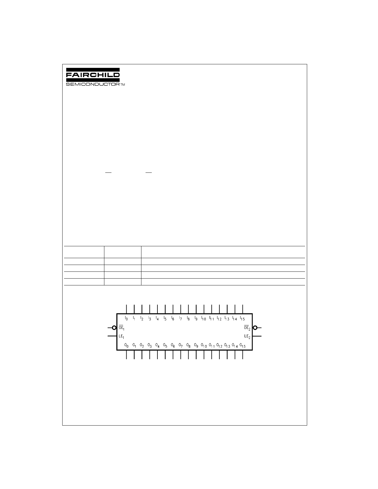
74LVT16373 • 74LVTH16373
Low Voltage 16-Bit Transparent Latch with
3-STATE Outputs
General Description
The LVT16373 and LVTH16373 contain sixteen non-invert-
ing latches with 3-STATE outputs and is intended for bus
oriented applications. The device is byte controlled. The
flip-flops appear transparent to the data when the Latch
Enable (LE) is HIGH. When LE is LOW, the data that meets
the setup time is latched. Data appears on the bus when
the Output Enable (OE) is LOW. When OE is HIGH, the
outputs are in a high impedance state.
The LVTH16373 data inputs include bushold, eliminating
the need for external pull-up resistors to hold unused
inputs.
These latches are designed for low-voltage (3.3V) VCC
applications, but with the capability to provide a TTL inter-
face to a 5V environment. The LVT16373 and LVTH16373
are fabricated with an advanced BiCMOS technology to
achieve high speed operation similar to 5V ABT while
maintaining a low power dissipation.
Features
s Input and output interface capability to systems at 5V
VCC
s Bushold data inputs eliminate the need for external pull-
up resistors to hold unused inputs (74LVTH16373), also
available without bushold feature (74LVT16373).
s Live insertion/extraction permitted
s Power Up/Down high impedance provides glitch-free
bus loading
s Outputs source/sink −32 mA/+64 mA
s Functionally compatible with the 74 series 16373
s Latch-up performance exceeds 500 mA
Ordering Code:
Order Number
Package
Number
Package Descripion
74LVT16373MEA
MS48A
48-Lead Small Shrink Outline Package (SSOP), JEDEC MO-118, 0.300” Wide
74LVT16373MTD
MTD48
48-Lead Thin Shrink Small Outline Package (TSSOP), JEDEC MO-153, 6.1mm Wide
74LVTH16373MEA
MS48A
48-Lead Small Shrink Outline Package (SSOP), JEDEC MO-118, 0.300” Wide
74LVTH16373MTD
MTD48
48-Lead Thin Shrink Small Outline Package (TSSOP), JEDEC MO-153, 6.1mm Wide
Device also available in Tape and Reel. Specify by appending suffix letter “X” to the ordering code.
Logic Symbol
© 1999 Fairchild Semiconductor Corporation DS012021.prf
www.fairchildsemi.com
1 page 
DC Electrical Characteristics (Continued)
Symbol
Parameter
IOZH+
ICCH
ICCL
ICCZ
ICCZ+
3-STATE Output Leakage Current
Power Supply Current
Power Supply Current
Power Supply Current
Power Supply Current
T A = −40°C to +85°C
VCC
(V)
Min
Typ Max Units
(Note 3)
3.6 10 µA
3.6
0.19
mA
3.6 5 mA
3.6
0.19
mA
3.6
0.19
mA
∆ICC
Increase in Power Supply Current
(Note 7)
3.6
0.2 mA
Note 3: All typical values are at VCC = 3.3V, TA = 25°C.
Note 4: Applies to bushold versions only (74LVTH16373).
Note 5: An external driver must source at least the specified current to switch from LOW to HIGH.
Note 6: An external driver must sink at least the specified current to switch from HIGH to LOW.
Note 7: This is the increase in supply current for each input that is at the specified voltage level rather than VCC or GND.
Conditions
VCC < VO ≤ 5.5V
Outputs HIGH
Outputs LOW
Outputs Disabled
VCC ≤ VO ≤ 5.5V,
Outputs Disabled
One Input at VCC − 0.6V
Other Inputs at VCC or GND
Dynamic Switching Characteristics (Note 8)
Symbol
Parameter
VCC TA = 25°C
(V) Min Typ Max
VOLP
Quiet Output Maximum Dynamic VOL
3.3
0.8
VOLV
Quiet Output Minimum Dynamic VOL
3.3
−0.8
Note 8: Characterized in SSOP package. Guaranteed parameter, but not tested.
Note 9: Max number of outputs defined as (n). n−1 data inputs are driven 0V to 3V. Output under test held LOW.
Units
V
V
Conditions
CL = 50 pF,
RL = 500Ω
(Note 9)
(Note 9)
AC Electrical Characteristics
TA = −40°C to +85°C, CL=50pF, RL=500Ω
Symbol
Parameter
VCC = 3.3V ±0.3V
Min
Typ
(Note 10) Max
VCC = 2.7V
Min Max
Units
tPHL Propagation Delay
1.5 3.9 1.5 4.3 ns
tPLH
Dn to On
1.5 3.8 1.5 4.2
tPHL Propagation Delay
1.9 4.2 1.9 4.4 ns
tPLH
LE to On
1.6 4.3 1.6 4.8
tPZL Output Enable Time 1.3 4.3 1.3 4.9 ns
tPZH 1.0 4.3 1.0 5.1
tPLZ Output Disable Time
1.5
4.7 1.5 4.8 ns
tPHZ 2.0 5.0 2.0 5.4
tS Setup Time, Dn to LE
1.0
0.8 ns
tH Hold Time, Dn to LE
1.0
1.1 ns
tW LE Pulse Width
3.0
3.0 ns
tOSHL
Output to Output Skew (Note 11)
1.0 1.0 ns
tOSLH
1.0 1.0
Note 10: All typical values are at VCC = 3.3V, TA = 25°C.
Note 11: Skew is defined as the absolute value of the difference between the actual propagation delay for any two separate outputs of the same device. The
specification applies to any outputs switching in the same direction, either HIGH to LOW (tOSHL) or LOW to HIGH (tOSLH).
Capacitance (Note 12)
Symbol
Parameter
Conditions
CIN Input Capacitance
VCC = Open, VI = 0V or VCC
COUT
Output Capacitance
VCC = 3.0V, VO = 0V or VCC
Note 12: Capacitance is measured at frequency f = 1 MHz, per MIL-STD-883, Method 3012.
Typical
4
8
Units
pF
pF
5 www.fairchildsemi.com
5 Page | ||
| Páginas | Total 7 Páginas | |
| PDF Descargar | [ Datasheet 74LVT16373MTD.PDF ] | |
Hoja de datos destacado
| Número de pieza | Descripción | Fabricantes |
| 74LVT16373MTD | Low Voltage 16-Bit Transparent Latch with 3-STATE Outputs | Fairchild Semiconductor |
| Número de pieza | Descripción | Fabricantes |
| SLA6805M | High Voltage 3 phase Motor Driver IC. |
Sanken |
| SDC1742 | 12- and 14-Bit Hybrid Synchro / Resolver-to-Digital Converters. |
Analog Devices |
|
DataSheet.es es una pagina web que funciona como un repositorio de manuales o hoja de datos de muchos de los productos más populares, |
| DataSheet.es | 2020 | Privacy Policy | Contacto | Buscar |