|
|
|
PDF 74VCXH16373 Data sheet ( Hoja de datos )
| Número de pieza | 74VCXH16373 | |
| Descripción | Low Voltage 16-Bit Transparent Latch with Bushold | |
| Fabricantes | Fairchild Semiconductor | |
| Logotipo | ||
Hay una vista previa y un enlace de descarga de 74VCXH16373 (archivo pdf) en la parte inferior de esta página. Total 8 Páginas | ||
|
No Preview Available !
74VCXH16245
Low−Voltage 1.8/2.5/3.3V
16−Bit Transceiver
With 3.6 V−Tolerant Inputs and Outputs
(3−State, Non−Inverting)
The 74VCXH16245 is an advanced performance, non−inverting
16−bit transceiver. It is designed for very high−speed, very low−power
operation in 1.8 V, 2.5 V or 3.3 V systems.
When operating at 2.5 V (or 1.8 V) the part is designed to tolerate
voltages it may encounter on either inputs or outputs when interfacing
to 3.3 V busses. It is guaranteed to be over−voltage tolerant to 3.6 V.
The VCXH16245 is designed with byte control. It can be operated
as two separate octals, or with the controls tied together, as a 16−bit
wide function. The Transmit/Receive (T/Rn) inputs determine the
direction of data flow through the bi−directional transceiver. Transmit
(active−HIGH) enables data from A ports to B ports; Receive
(active−LOW) enables data from B to A ports. The Output Enable
inputs (OEn), when HIGH, disable both A and B ports by placing them
in a HIGH Z condition. The data inputs include active bushold
circuitry, eliminating the need for external pull−up resistors to hold
unused or floating inputs at a valid logic state.
Features
• Designed for Low Voltage Operation: VCC = 1.65−3.6 V
• 3.6 V Tolerant Inputs and Outputs
• High Speed Operation: 2.5 ns max for 3.0 to 3.6 V
3.0 ns max for 2.3 to 2.7 V
6.0 ns max for 1.65 to 1.95 V
• Static Drive: ±24 mA Drive at 3.0 V
±18 mA Drive at 2.3 V
±6 mA Drive at 1.65 V
• Supports Live Insertion and Withdrawal
• Includes Active Bushold to Hold Unused or Floating Inputs at a Valid
Logic State
• IOFF Specification Guarantees High Impedance When VCC = 0 V*
• Near Zero Static Supply Current in All Three Logic States (20 mA)
Substantially Reduces System Power Requirements
• Latchup Performance Exceeds ±250 mA @ 125°C
• ESD Performance: Human Body Model >2000 V;
Machine Model >200 V
• Pb−Free Package is Available*
*NOTE: To ensure the outputs activate in the 3−state condition,
the output enable pins should be connected to VCC through a
pull−up resistor. The value of the resistor is determined by the
current sinking capability of the output connected to the OE pin.
http://onsemi.com
48
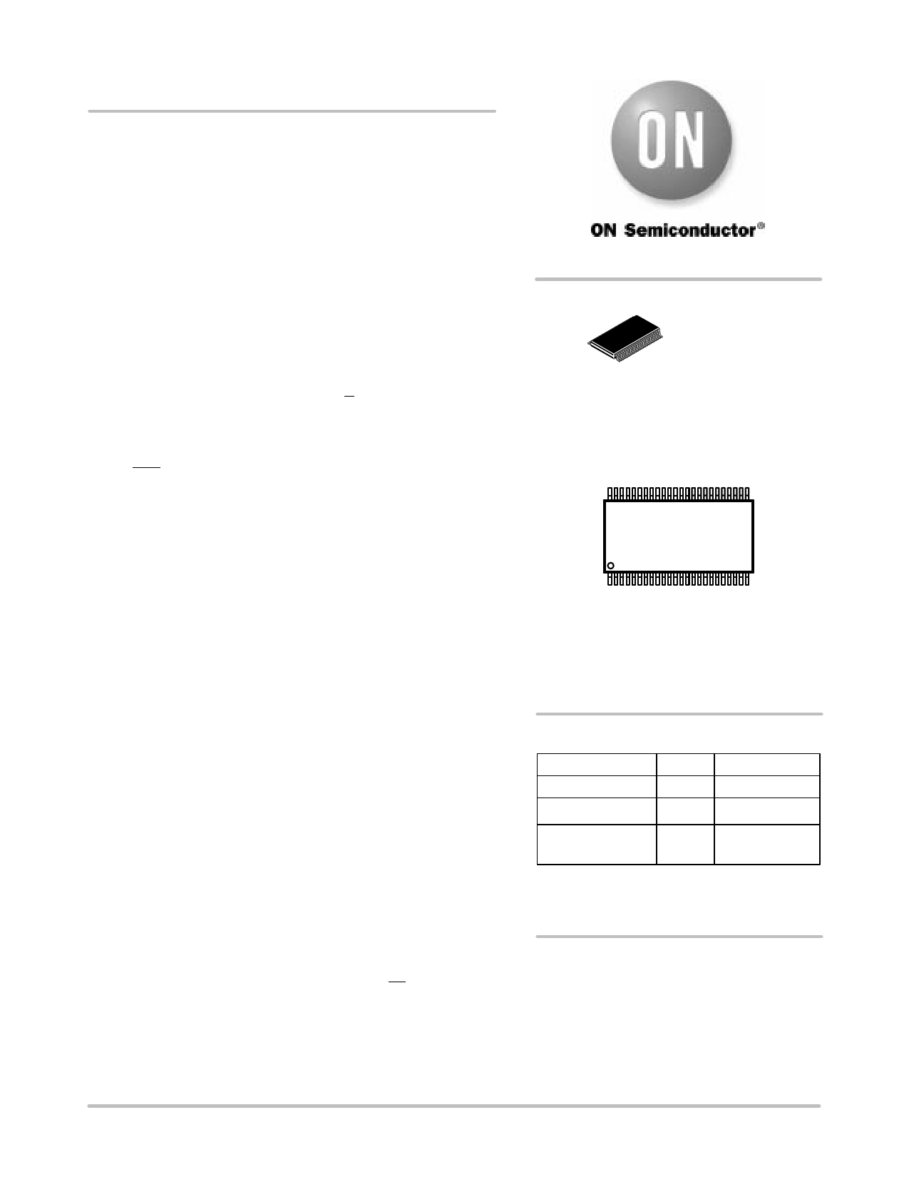
1
TSSOP−48
DT SUFFIX
CASE 1201
MARKING DIAGRAM
48
VCXH16245
AWLYYWW
1
A = Assembly Location
WL = Wafer Lot
YY = Year
WW = Work Week
ORDERING INFORMATION
Device
Package
Shipping†
74VCXH16245DT TSSOP
39 / Rail
74VCXH16245DTR TSSOP 2500/Tape & Reel
74VCXH16245DTRG TSSOP 2500/Tape & Reel
(Pb−Free)
†For information on tape and reel specifications,
including part orientation and tape sizes, please
refer to our Tape and Reel Packaging Specification
Brochure, BRD8011/D.
*For additional information on our Pb−Free strategy
and soldering details, please download the
ON Semiconductor Soldering and Mounting
Techniques Reference Manual, SOLDERRM/D.
© Semiconductor Components Industries, LLC, 2004
May, 2004 − Rev. 3
1
Publication Order Number:
74VCXH16245/D
1 page 
74VCXH16245
AC CHARACTERISTICS (Note 6.; tR = tF = 2.0ns; CL = 30pF; RL = 500W)
Limits
Symbol
Parameter
Waveform
VCC = 3.0 V to 3.6 V
Min Max
TA = −40°C to +85°C
VCC = 2.3 V to 2.7 V
Min Max
VCC = 1.65 to1.95 V
Min Max
Unit
tPLH Propagation Delay
tPHL Input to Output
1 0.8 2.5 1.0 3.0 1.5 6.0 ns
0.8 2.5 1.0 3.0 1.5 6.0
tPZH
tPZL
Output Enable Time to
High and Low Level
2 0.8 3.8 1.0 4.9 1.5 9.3 ns
0.8 3.8 1.0 4.9 1.5 9.3
tPHZ
tPLZ
Output Disable Time From
High and Low Level
2 0.8 3.7 1.0 4.2 1.5 7.6 ns
0.8 3.7 1.0 4.2 1.5 7.6
tOSHL
tOSLH
Output−to−Output Skew
(Note 7.)
0.5 0.5 0.75 ns
0.5 0.5 0.75
6. For CL = 50pF, add approximately 300ps to the AC maximum specification.
7. Skew is defined as the absolute value of the difference between the actual propagation delay for any two separate outputs of the same device.
The specification applies to any outputs switching in the same direction, either HIGH−to−LOW (tOSHL) or LOW−to−HIGH (tOSLH); parameter
guaranteed by design.
DYNAMIC SWITCHING CHARACTERISTICS
Symbol
Characteristic
Condition
TA = +25°C
Typ
Unit
VOLP
Dynamic LOW Peak Voltage
VCC = 1.8 V, CL = 30pF, VIH = VCC, VIL = 0 V
0.25
V
(Note 8.)
VCC = 2.5 V, CL = 30pF, VIH = VCC, VIL = 0 V
0.6
VCC = 3.3 V, CL = 30pF, VIH = VCC, VIL = 0 V
0.8
VOLV
Dynamic LOW Valley Voltage
VCC = 1.8 V, CL = 30pF, VIH = VCC, VIL = 0 V
−0.25
V
(Note 8.)
VCC = 2.5 V, CL = 30pF, VIH = VCC, VIL = 0 V
−0.6
VCC = 3.3 V, CL = 30pF, VIH = VCC, VIL = 0 V
−0.8
VOHV Dynamic HIGH Valley Voltage
VCC = 1.8 V, CL = 30pF, VIH = VCC, VIL = 0 V
1.5
V
(Note 9.)
VCC = 2.5 V, CL = 30pF, VIH = VCC, VIL = 0 V
1.9
VCC = 3.3 V, CL = 30pF, VIH = VCC, VIL = 0 V
2.2
8. Number of outputs defined as “n”. Measured with “n−1” outputs switching from HIGH−to−LOW or LOW−to−HIGH. The remaining output is
measured in the LOW state.
9. Number of outputs defined as “n”. Measured with “n−1” outputs switching from HIGH−to−LOW or LOW−to−HIGH. The remaining output is
measured in the HIGH state.
CAPACITIVE CHARACTERISTICS
Symbol
Parameter
Condition
Typical
Unit
CIN
COUT
CPD
Input Capacitance
Output Capacitance
Power Dissipation Capacitance
Note 10.
Note 10.
Note 10., 10MHz
6 pF
7 pF
20 pF
10. VCC = 1.8, 2.5 or 3.3 V; VI = 0 V or VCC.
AC CHARACTERISTICS (tR = tF = 2.0ns; CL = 50pF; RL = 500W)
Limits
Symbol
Parameter
Waveform
TA = −40°C to +85°C
VCC = 3.0 V to 3.6 V
VCC = 2.7 V
Min Max Min Max
Unit
tPLH Propagation Delay
tPHL Input to Output
3 1.0 3.0
1.0 3.0
3.6 ns
3.6
tPZH
tPZL
Output Enable Time to
High and Low Level
4 1.0 4.4
1.0 4.4
5.4 ns
5.4
tPHZ
tPLZ
Output Disable Time From
High and Low Level
4 1.0 4.1
1.0 4.1
4.6 ns
4.6
tOSHL
tOSLH
Output−to−Output Skew
(Note 11.)
0.5 0.5 ns
0.5 0.5
11. Skew is defined as the absolute value of the difference between the actual propagation delay for any two separate outputs of the same device.
The specification applies to any outputs switching in the same direction, either HIGH−to−LOW (tOSHL) or LOW−to−HIGH (tOSLH); parameter
guaranteed by design.
http://onsemi.com
5
5 Page | ||
| Páginas | Total 8 Páginas | |
| PDF Descargar | [ Datasheet 74VCXH16373.PDF ] | |
Hoja de datos destacado
| Número de pieza | Descripción | Fabricantes |
| 74VCXH16373 | Low Voltage 16-Bit Transparent Latch with Bushold | Fairchild Semiconductor |
| 74VCXH16373 | Low-Voltage 1.8/2.5/3.3 V 16-Bit Transparent Latch | ON Semiconductor |
| 74VCXH16374 | Low Voltage 16-Bit D-Type Flip-Flop with Bushold | Fairchild Semiconductor |
| 74VCXH16374 | LOW VOLTAGE CMOS 16-BIT D-TYPE FLIP-FLOP | ST Microelectronics |
| Número de pieza | Descripción | Fabricantes |
| SLA6805M | High Voltage 3 phase Motor Driver IC. |
Sanken |
| SDC1742 | 12- and 14-Bit Hybrid Synchro / Resolver-to-Digital Converters. |
Analog Devices |
|
DataSheet.es es una pagina web que funciona como un repositorio de manuales o hoja de datos de muchos de los productos más populares, |
| DataSheet.es | 2020 | Privacy Policy | Contacto | Buscar |