|
|
PDF M7232 Data sheet ( Hoja de datos )
| Número de pieza | M7232 | |
| Descripción | Numeric/Alphanumeric Triplexed LCD Display Drivers | |
| Fabricantes | Intersil | |
| Logotipo |  |
|
Hay una vista previa y un enlace de descarga de M7232 (archivo pdf) en la parte inferior de esta página. Total 16 Páginas | ||
|
No Preview Available !
ICM7231, ICM7232
August 1997
Numeric/Alphanumeric Triplexed
LCD Display Drivers
Features
Description
• ICM7231 Drives 8 Digits of 7 Segments with Two
Independent Annunciators Per Digit Address and Data
Input in Parallel Format
• ICM7232 Drives 10 Digits of 7 Segments with Two
Independent Annunciators Per Digit Address and Data
Input in Serial Format
• All Signals Required to Drive Rows and Columns of
Triplexed LCD Display are Provided
• Display Voltage Independent of Power Supply
• On-Chip Oscillator Provides All Display Timing
The ICM7231 and ICM7232 family of integrated circuits are
designed to generate the voltage levels and switching wave-
forms required to drive triplexed liquid-crystal displays.
These chips also include input buffer and digit address
decoding circuitry allowing six bits of input data to be
decoded into 64 independent combinations of the output
segments of the selected digit.
The family is designed to interface to modern high-
performance microprocessors and microcomputers and
ease system requirements for ROM space and CPU time
needed to service a display.
• Total Power Consumption Typically 200µW, Maximum
500µW at 5V
• Low-Power Shutdown Mode Retains Data With 5µW
Typical Power Consumption at 5V, 1µW at 2V
• Direct Interface to High-Speed Microprocessors
Ordering Information
PART NUMBER
TEMP. RANGE (oC)
PACKAGE
ICM7231BFIJL
-25 to 85
40 Ld CERDIP
ICM7231BFIPL
-25 to 85
40 Ld PDIP
ICM7232BFIPL
-25 to 85
40 Ld PDIP
ICM7232CRIPL
-25 to 85
40 Ld PDIP
NOTE:
All versions intended for triplexed LCD displays.
NUMBER OF DIGITS
8 Digit
8 Digit
10 Digit
10 Digit
INPUT FORMAT
Parallel
Parallel
Serial
Serial
PKG. NO.
F40.6
E40.6
E40.6
E40.6
CAUTION: These devices are sensitive to electrostatic discharge; follow proper IC Handling Procedures.
http://www.intersil.com or 407-727-9207 | Copyright © Intersil Corporation 1999
9-19
File Number 3161.1
1 page 
ICM7231, ICM7232
Absolute Maximum Ratings
Supply Voltage (VDD - VSS) . . . . . . . . . . . . . . . . . . . . . . . . . . . . 6.5V
Input Voltage (Note 1). . . . . . . . . . . . . . . . . . . . VSS - 0.3 ≤ VIN ≤ 6.5
Display Voltage (Note 1) . . . . . . . . . . . . . . . . . . . .0.3 ≤ VDISP ≤ +0.3
Operating Conditions
Temperature Range . . . . . . . . . . . . . . . . . . . . . . . . . . -25oC to 85oC
Thermal Information
Thermal Resistance (Typical, Note 2)
θJA (oC/W) θJC (oC/W)
PDIP Package . . . . . . . . . . . . . . . . . . .
60
N/A
CERDIP Package . . . . . . . . . . . . . . . .
50
12
Maximum Junction Temperature
Ceramic Package . . . . . . . . . . . . . . . . . . . . . . . . . . . . . . . . 175oC
Plastic Package . . . . . . . . . . . . . . . . . . . . . . . . . . . . . . . . . . 150oC
Maximum Storage Temperature Range . . . . . . . . . .-65oC to 150oC
Maximum Lead Temperature (Soldering, 10s) . . . . . . . . . . . . 300oC
CAUTION: Stresses above those listed in “Absolute Maximum Ratings” may cause permanent damage to the device. This is a stress only rating and operation
of the device at these or any other conditions above those indicated in the operational sections of this specification is not implied.
NOTES:
1. Due to the SCR structure inherent in these devices, connecting any display terminal or the display voltage terminal to a voltage outside
the power supply to the chip may cause destructive device latchup. The digital inputs should never be connected to a voltage less than
-0.3V below ground, but maybe connected to voltages above VDD but not more than 6.5V above VSS.
2. θJA is measured with the component mounted on an evaluation PC board in free air.
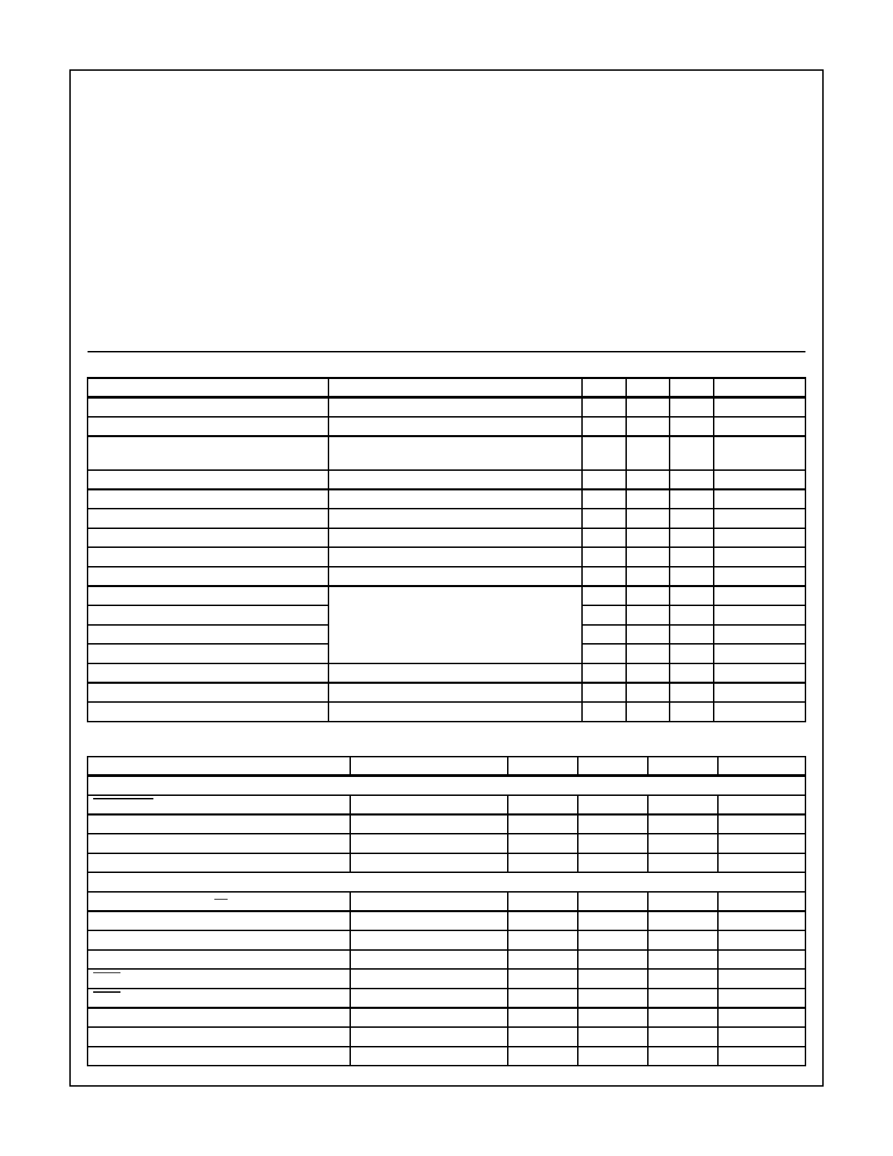
Electrical Specifications V+ = 5V +10%, VSS = 0V, TA = -25oC to 85oC, Unless Otherwise Specified
PARAMETER
TEST CONDITIONS
MIN TYP
Power Supply Voltage, VDD
Data Retention Supply Voltage, VDD
Logic Supply Current, IDD
Shutdown Total Current, IS
Display Voltage Range, VDISP
Display Voltage Setup Current, IDISP
Display Voltage Setup Resistor Value, RDISP
DC Component of Display Signals
Guaranteed Retention at 2V
Current from VDD to Ground Excluding Display.
VDISP = 2V
VDISP Pin 2 Open
VSS ≤ VDISP ≤ VDD
VDISP = 2V, Current from VDD to VDISP On-Chip
One of Three Identical Resistors in String
(Sample Test Only)
Display Frame Rate, fDISP
Input Low Level, VIL
Input High Level, VIH
Input Leakage, IILK
Input Capacitance, CIN
Output Low Level, VOL
Output High Level, VOH
Operating Temperature Range, TOP
See Figure 5
ICM7231, Pins 30 - 35, 37 - 39, 1
ICM7232, Pins 1, 38, 39 (Note 2)
Pin 37, ICM7232, IOL = 1mA
VDD = 4.5V, IOH = -500µA
Industrial Range
4.5
2
-
-
0
-
40
-
60
-
2.0
-
-
-
4.1
-25
>4
1.6
30
1
-
15
75
1/4
90
-
-
0.1
5
-
-
-
MAX
5.5
-
100
UNITS
V
V
µA
10
VDD
30
-
1
120
0.8
-
1
-
0.4
-
+85
µA
V
µA
kΩ
% (VDD - VDISP)
Hz
V
V
µA
pF
V
V
oC
AC Specifications VDD = 5V +10% VSS = 0V, -25oC to 85oC
PARAMETER
TEST CONDITIONS MIN TYP MAX UNITS
PARALLEL INPUT (ICM7231) See Figure 1
Chip Select Pulse Width, tCS
Address/Data Setup Time, tDS
Address/Data Hold Time, tDH
Inter-Chip Select Time, tICS
SERIAL INPUT (ICM7232) See Figures 2, 3
(Note 1)
(Note 1)
(Note 1)
(Note 1)
500 350
200 -
0 -20
3-
-
-
-
-
ns
ns
ns
µs
Data Clock Low Time, tCL
Data Clock High Time, tCL
Data Setup Time, tDS
Data Hold Time, tDH
Write Pulse Width, tWP
Write Pulse to Clock at Initialization, tWLL
Data Accepted Low Output Delay, tODL
Data Accepted High Output Delay, tODH
Write Delay After Last Clock, tCWS
(Note 1)
(Note 1)
(Note 1)
(Note 1)
(Note 1)
(Note 1)
(Note 1)
(Note 1)
(Note 1)
350 -
-
350 -
-
200 -
-
0 -20 -
500 350
-
1.5 -
-
- 200 400
- 1.5 3
350 -
-
ns
ns
ns
ns
ns
µs
ns
µs
ns
9-23
5 Page 
ICM7231, ICM7232
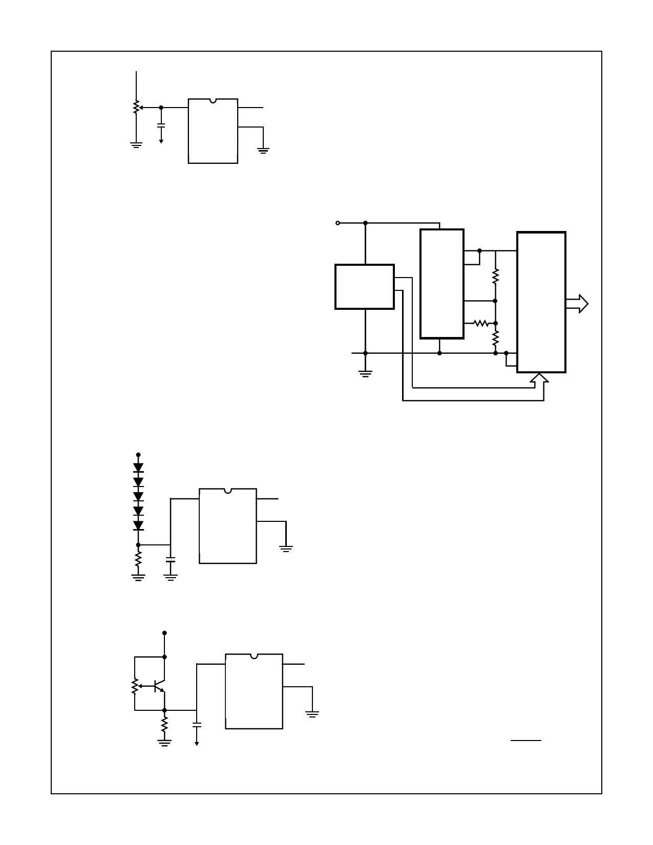
OPEN
200kΩ
2 VDISP 40
10nF
36
ICM7231
ICM7232
+5
FIGURE 10. SIMPLE DISPLAY VOLTAGE ADJUSTMENT
Figure 11A shows another method of setting up a display
voltage using five silicon diodes in series. These diodes,
1N914 or equivalent, will each have a forward drop of
approximately 0.65V, with approximately 20µA flowing
through them at room temperature. Thus, 5 diodes will give
3.25V, suitable for a 3V display using the material properties
shown in Figures 4 and 5. For higher voltage displays, more
diodes may be added. This circuit provides reasonable
temperature compensation, as each diode has a negative
temperature coefficient of -2mV/oC; five in series gives
-10mV/oC, not far from optimum for the material described.
The disadvantage of the diodes in series is that only integral
multiples of the diode voltage can be achieved. The diode
voltage multiplier circuit shown in Figure 11B allows fine-
tuning the display voltage by means of the potentiometer; it
likewise provides temperature compensation since the tem-
perature coefficient of the transistor base-emitter junction
(about -2mV/oC) is also multipled. The transistor should have
a beta of at least 100 with a collector current of 10µA. The
inexpensive 2N2222 shown in the figure is a suitable device.
VDD
1N914
DIODES
40kΩ
2 VDISP 40
36
ICM7231
ICM7232
10nF
+5
FIGURE 11A. STRING OF DIODES
VDD
200kΩ
POTENTIOMETER
2N2222
2 VDISP 40
36
ICM7231
ICM7232
40kΩ
10nF
+5
FIGURE 11B. TRANSISTOR-MULTIPLIER
FIGURE 11. DIODE-BASED TEMPERATURE COMPENSATION
For battery operation, where the display voltage is generally the
same as the battery voltage (usually 3 - 4.5V), the chip may be
operated at the display voltage, with VDlSP connected to VSS.
The inputs of the chip are designed such that they may be
driven above VDD without damaging the chip. This allows, for
example, the chip and display to operate at a regulated 3V, and
a microprocessor driving its inputs to operate with a less well
controlled 5V supply. (The inputs should not be driven more
than 6.5V above GND under any circumstances.) This also
allows temperature compensation with the ICL7663S, as
shown in Figure 12. This circuit allows independent adjustment
of both voltage and temperature compensation.
+5V
LOGIC
SYSTEM
PROCESSOR,
ETC.
VIN +
VOUT1
VOUT2
1.8MΩ
ICL7663S
VSET
VTC
GND
300kΩ
2.7MΩ
VDD
ICM7233
VDISP
GND
DATA BUS
FIGURE 12. FLEXIBLE TEMPERATURE COMPENSATION
Description Of Operation
Parallel Input Of Data And Address (ICM7231)
The parallel input structure of the ICM7231 device is
organized to allow simple, direct interfacing to all micropro-
cessors, (see the Functional Block Diagram). In the
ICM7231, address and data bits are written into the input
latches on the rising edge of the Chip Select input.
The rising edge of the Chip Select also triggers an on-chip
pulse which enables the address decoder and latches the
decoded data into the addressed digit/character outputs. The
timing requirements for the parallel input device are shown in
Figure 1, with the values for setup, hold, and pulse width times
shown in the AC Specifications section. Note that there is a
minimum time between Chip Select pulses; this is to allow suf-
ficient time for the on-chip enable pulse to decay, and ensures
that new data doesn’t appear at the decoder inputs before the
decoded data is written to the outputs.
Serial Input Of Data And Address (ICM7232)
The ICM3232 trades six pins used as data inputs on the
ICM7231 for six more segment lines, allowing two more
9-segment digits. This is done at the cost of ease in interfac-
ing, and requires that data and address information be
entered serially. Refer to Functional Block Diagram and tim-
ing diagrams, Figures 2 and 3. The interface consists of four
pins: DATA Input, DATA CLOCK Input, WRITE Input and
DATA ACCEPTED Output. The data present at the DATA
Input is clocked into a shift register on the rising edge of the
9-29
11 Page | ||
| Páginas | Total 16 Páginas | |
| PDF Descargar | [ Datasheet M7232.PDF ] | |
Hoja de datos destacado
| Número de pieza | Descripción | Fabricantes |
| M7232 | Numeric/Alphanumeric Triplexed LCD Display Drivers | Intersil |
| M7232 | CONTINUOUS / ON/OFF LIGHT DIMMER | ETC |
| Número de pieza | Descripción | Fabricantes |
| SLA6805M | High Voltage 3 phase Motor Driver IC. |
Sanken |
| SDC1742 | 12- and 14-Bit Hybrid Synchro / Resolver-to-Digital Converters. |
Analog Devices |
|
DataSheet.es es una pagina web que funciona como un repositorio de manuales o hoja de datos de muchos de los productos más populares, |
| DataSheet.es | 2020 | Privacy Policy | Contacto | Buscar |
