|
|
|
PDF M902-01 Data sheet ( Hoja de datos )
| Número de pieza | M902-01 | |
| Descripción | VCSO BASED GBE CLOCK GENERATOR | |
| Fabricantes | Integrated Circuit Systems | |
| Logotipo | ||
Hay una vista previa y un enlace de descarga de M902-01 (archivo pdf) en la parte inferior de esta página. Total 8 Páginas | ||
|
No Preview Available !
Integrated
Circuit
Systems, Inc.
Product Data Sheet
M902-01
VCSO BASED GBE CLOCK GENERATOR
GENERAL DESCRIPTION
The M902-01 is a PLL (Phase Locked Loop) based
clock generator that uses an
internal VCSO (Voltage Controlled
SAW Oscillator) to produce a very
low jitter output clock. It is ideal for
Gigabit Ethernet. The output clock
(frequency of 156.25 or 187.50MHz
for example) is provided from two
LVPECL clock output pairs. (Specify frequency at time
of order.) The accuracy of the output frequency is
assured by the internal PLL, which phase-locks the
internal VCSO to the reference input frequency (25 or
30MHz for example). The input reference can either
be an external crystal, utilizing the internal crystal
oscillator, or a stable external clock source such as
a packaged crystal oscillator.
FEATURES
◆ Output clock frequency from 125MHz to 190MHz
(Consult factory for frequency availability)
◆ Two identical LVPECL output pairs
◆ Integrated SAW (surface acoustic wave) delay line
◆ Low jitter 0.5ps rms (over 12kHz-20MHz)
◆ Ideal for Gigabit Ethernet clock reference
◆ Output-to-output skew < 100ps
◆ External XTAL or LVCMOS reference input
◆ Selectable external feed-through clock input
◆ STOP clock control (Logic 1 stops output clocks)
◆ Industrial temperature grade available
◆ Single 3.3V power supply
◆ Small 9 x 9 mm SMT (surface mount) package
SIMPLIFIED BLOCK DIAGRAM
M902-01
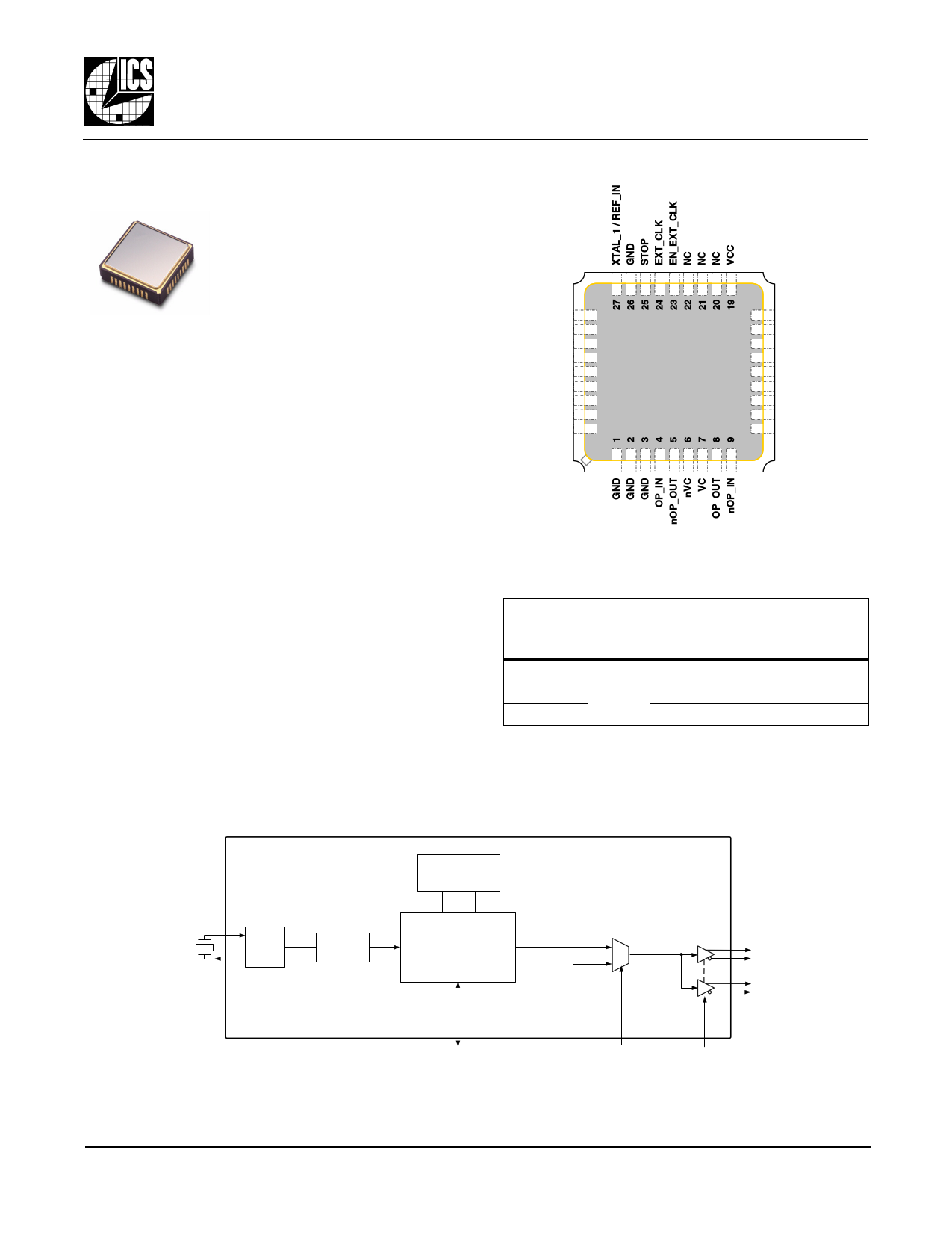
PIN ASSIGNMENT (9 x 9 mm SMT)
XTAL_2
NC
NC
NC
NC
VCC
DNC
DNC
DNC
28 18
29 17
30 16
31 M 9 0 2 - 0 1 15
32 14
33 ( T o p V i e w ) 13
34 12
35 11
36 10
NC
NC
nFOUT1
FOUT1
GND
nFOUT0
FOUT0
VCC
GND
Figure 1: Pin Assignment
Example Output Frequency Configurations
Ref Clock
Frequency
(MHz)
PLL
Ratio
Output
Frequency 1
(MHz)
Application
20
125.00
GbE
25 25/4 156.25
10GbE
30
187.50
12GbE
Table 1: Example Output Frequency Configurations
Note 1: Specify output clock frequency at time of order
VSCO
External
Crystal
or
Reference
Clock Input
(e.g., 25 or 30MHz)
XTAL
OSC
Divider
Frequency
Multiplying
PLL
O
1
LVPECL
Output
Clock Pairs
(e.g., 156.25
or 187.50MHz)
External
Loop Filter
External
Clock
Input
External Output
Clock Clock STOP
Select
Control
Figure 2: Simplified Block Diagram
M902-01 Datasheet Rev 2.1
Revised 24Jun2004
M902-01 VCSO Based GbE Clock Generator
Integrated Circuit Systems, Inc. ● Networking & Communications ● www.icst.com ● tel (508) 852-5400
1 page 
Integrated
Circuit
Systems, Inc.
PLL Simulator Tool Available
A free PC software utility is available on the ICS website
(www.icst.com). The M2000 Timing Modules PLL
Simulator is a downloadable application that simulates
PLL jitter and wander transfer characteristics. This
enables the user to set appropriate external loop
component values in a given application.
Refer to the SAW PLL Simulator Software web page at
www.icst.com/products/calculators/m2000filterSWdesc.htm
for additional information.
M902-01
VCSO BASED GBE CLOCK GENERATOR
Product Data Sheet
SAW PLL Application Notes Available
The ICS web site (www.icst.com) also has application
notes on:
• PCB layout guidelines (including special detailed
instructions for preventing issues such as external
reference crosstalk)
• Any new special device application details that may
become available
• Instructions for using PLL simulator software
• Guidelines for PCB fabrication (including recom-
mended PCB footprint, solder mask, and furnace
profile)
Refer to the SAW PLL Application Notes web page at
www.icst.com/products/appnotes/SawPllAppNotes.htm
for application notes and any additional product
information that may become available.
ABSOLUTE MAXIMUM RATINGS1
Symbol Parameter
Rating
Unit
VI Input Voltage
-0.5 to VCC +0.5
V
VO Output Voltage
-0.5 to VCC +0.5
V
I O Output Current
25 mA
VCC Power Supply Voltage
TS Storage Temperature
4.6
-45 to +100
V
oC
Table 5: Absolute Maximum Ratings
Note 1: Stresses beyond those listed under Absolute Maximum Ratings may cause permanent damage to the
device. These ratings are stress specifications only. Functional operation of product at these conditions
or any conditions beyond those listed in Recommended Conditions of Operation, DC Characteristics, or
AC Characteristics is not implied. Exposure to absolute maximum rating conditions for extended periods
may affect product reliability.
RECOMMENDED CONDITIONS OF OPERATION
Symbol Parameter
Min Typ Max Unit
VCC Positive Supply Voltage
3.135 3.3 3.465 V
TA Ambient Operating Temperature
Commercial
0
+70 oC
Industrial
-40
+85 oC
Table 6: Recommended Conditions of Operation
M902-01 Datasheet Rev 2.1
5 of 8
Revised 24Jun2004
Integrated Circuit Systems, Inc. ● Networking & Communications ● www.icst.com ● tel (508) 852-5400
5 Page | ||
| Páginas | Total 8 Páginas | |
| PDF Descargar | [ Datasheet M902-01.PDF ] | |
Hoja de datos destacado
| Número de pieza | Descripción | Fabricantes |
| M902-01 | VCSO BASED GBE CLOCK GENERATOR | Integrated Circuit Systems |
| Número de pieza | Descripción | Fabricantes |
| SLA6805M | High Voltage 3 phase Motor Driver IC. |
Sanken |
| SDC1742 | 12- and 14-Bit Hybrid Synchro / Resolver-to-Digital Converters. |
Analog Devices |
|
DataSheet.es es una pagina web que funciona como un repositorio de manuales o hoja de datos de muchos de los productos más populares, |
| DataSheet.es | 2020 | Privacy Policy | Contacto | Buscar |