|
|
PDF OQ2541HP Data sheet ( Hoja de datos )
| Número de pieza | OQ2541HP | |
| Descripción | SDH/SONET data and clock recovery unit STM1/4/16 OC3/12/48 GE | |
| Fabricantes | NXP Semiconductors | |
| Logotipo | ||
Hay una vista previa y un enlace de descarga de OQ2541HP (archivo pdf) en la parte inferior de esta página. Total 30 Páginas | ||
|
No Preview Available !
INTEGRATED CIRCUITS
DATA SHEET
OQ2541HP; OQ2541U
SDH/SONET data and clock
recovery unit STM1/4/16
OC3/12/48 GE
Product specification
Supersedes data of 1999 Mar 19
File under Integrated Circuits, IC19
1999 May 27
1 page 
Philips Semiconductors
SDH/SONET data and clock recovery unit
STM1/4/16 OC3/12/48 GE
Product specification
OQ2541HP; OQ2541U
SYMBOL PIN
DESCRIPTION
GND
DOUT
DOUTQ
GND
COUT
COUTQ
GND
AREF
41 ground; note 1
42 data output in normal mode (differential)
43 inverted data output in normal mode (differential)
44 ground; note 1
45 clock output in normal mode (differential)
46 inverted clock output in normal mode (differential)
47 ground; note 1
48 reference voltage input for controlling voltage swing on data and clock outputs
Notes
1. ALL GND pins or pads must be bonded; do not leave one single GND pin or pad unconnected.
2. ALL pins or pads denoted ‘i.c.’ should not be connected. Connections to these pins or pads degrade device
performance.
3. ALL VEE pins or pads must be bonded; do not leave one single VEE pin or pad unconnected.
handbook, full pagewidth
ENL 1
GND 2
CLOOP 3
CLOOPQ 4
GND 5
DLOOP 6
DLOOPQ 7
GND 8
DREF19 9
GND 10
GND 11
LOCK 12
OQ2541HP
36 i.c.
35 GND
34 DINQ
33 DIN
32 GND
31 VEE2
30 DOUT155
29 GND
28 DOUT622
27 DOUT1250
26 GND
25 VEE1
MBH971
1999 May 27
Fig.2 Pin configuration.
5
5 Page 
Philips Semiconductors
SDH/SONET data and clock recovery unit
STM1/4/16 OC3/12/48 GE
Product specification
OQ2541HP; OQ2541U
Application with positive supply voltage
Due to the versatile design of the OQ2541 the device can
also operate in a positive supply voltage application,
although some pins have a different mode of operation.
This section deals with these differences and supports the
user with achieving a successful application of the
OQ2541 in a +5 V environment.
APPLICATION DIAGRAM
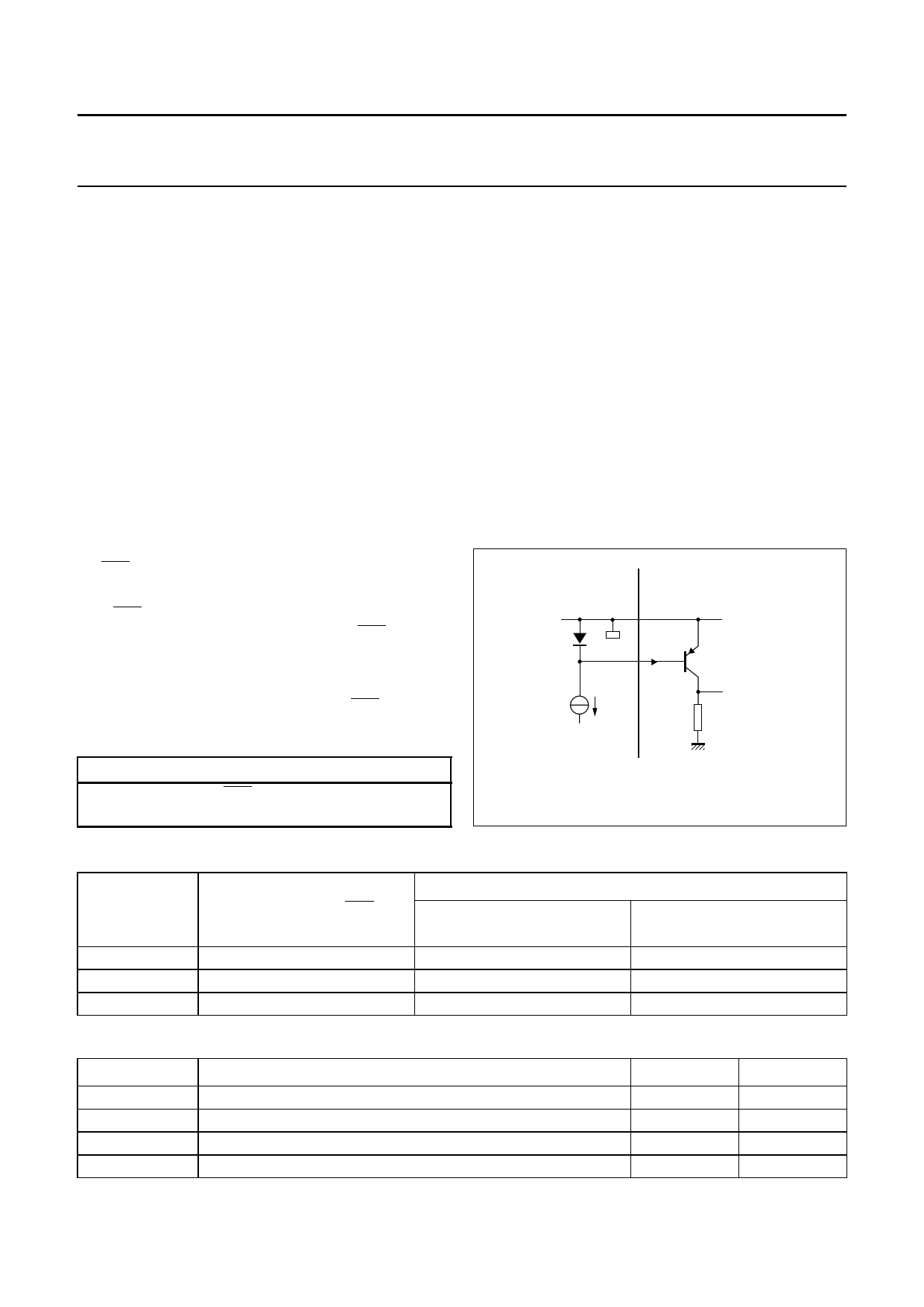
A sample application diagram can be found in Fig.29.
It should be noted that all pins GND are now connected to
VCC and all pins VEE are connected to the regulated
voltage from the power controller.
OUTPUT SELECTION
In a positive supply voltage application, the loop mode is
the default RF output. Due to the decoding logic on
pin ENL, it is only possible to select the loop mode outputs
or enable all the outputs.
If pin ENL is connected to VCC (+5 V), only the loop mode
outputs are active (see Table 4). When pin ENL is
connected to VEE (the voltage is approximately 3.3 V
below VCC) all outputs become active. In the positive
supply voltage application the normal mode outputs can
not be selected, unless the voltage on pin ENL is 2 V
above the positive supply voltage (VCC).
CAUTION
Do not to connect pin ENL to ground, because this will
destroy the IC.
LOSS OF SIGNAL AND LOCK DETECTION
In the negative supply application, pins LOS and LOCK
are open-collector outputs that require pull-up resistors to
a positive supply voltage.
In the positive supply application, the pull-up voltage would
need to be higher then the positive supply voltage and the
signals on pins LOS and LOCK would not be TTL
compatible any more. However, the internal circuit on
pins LOS and LOCK can be used in a current mirror
configuration (see Fig.9). This requires only an external
PNP transistor (e.g. BC857 or equivalent) to mirror the
current. A 10 kΩ pull-down resistor from the collector of the
external transistor to ground yields a TTL compatible
signal again, albeit inverted. Table 5 shows the meaning of
the LOS and LOCK flag, when used in the positive supply
application.
handbook, halfpage on chip
off chip
GND
+5 V
LOS,
LOCK
BC857
signal out
10 kΩ
MGL671
Fig.9 Signal out for LOS and LOCK indication in a
positive supply voltage application.
Table 4 Output selection in a positive supply voltage application
MODE
Loop
Loop and normal
Normal
LEVEL ON PIN ENL
VCC (+5 V)
VEE (VCC − 3.3 V)
VCC + 2 V
OUTPUT
DLOOP, DLOOPQ,
CLOOP AND CLOOPQ
active
active
−
DOUT, DOUTQ,
COUT AND COUTQ
−
active
active
Table 5 LOS and LOCK indication in a positive supply voltage application
SIGNAL
LOS active
LOS inactive
LOCK active
LOCK inactive
DESCRIPTION
loss of signal: BER > 5 ⋅ 10−2
no loss of signal: BER < 1 ⋅ 10−3
reference clock present and VCRO inside 1000 ppm window
no reference clock present or VCRO outside 1000 ppm window
LEVEL
0 V (ground)
+5 V (VCC)
0 V (ground)
+5 V (VCC)
TTL
LOW
HIGH
LOW
HIGH
1999 May 27
11
11 Page | ||
| Páginas | Total 30 Páginas | |
| PDF Descargar | [ Datasheet OQ2541HP.PDF ] | |
Hoja de datos destacado
| Número de pieza | Descripción | Fabricantes |
| OQ2541HP | SDH/SONET data and clock recovery unit STM1/4/16 OC3/12/48 GE | NXP Semiconductors |
| Número de pieza | Descripción | Fabricantes |
| SLA6805M | High Voltage 3 phase Motor Driver IC. |
Sanken |
| SDC1742 | 12- and 14-Bit Hybrid Synchro / Resolver-to-Digital Converters. |
Analog Devices |
|
DataSheet.es es una pagina web que funciona como un repositorio de manuales o hoja de datos de muchos de los productos más populares, |
| DataSheet.es | 2020 | Privacy Policy | Contacto | Buscar |
