|
|
|
PDF ST24C02 Data sheet ( Hoja de datos )
| Número de pieza | ST24C02 | |
| Descripción | SERIAL 2K (256 x 8) EEPROM | |
| Fabricantes | ST Microelectronics | |
| Logotipo | ||
Hay una vista previa y un enlace de descarga de ST24C02 (archivo pdf) en la parte inferior de esta página. Total 16 Páginas | ||
|
No Preview Available !
ST24/25C02, ST24C02R
ST24/25W02
SERIAL 2K (256 x 8) EEPROM
1 MILLION ERASE/WRITE CYCLES with
40 YEARS DATA RETENTION
SINGLE SUPPLY VOLTAGE:
– 3V to 5.5V for ST24x02 versions
– 2.5V to 5.5V for ST25x02 versions
– 1.8V to 5.5V for ST24C02R version only
HARDWARE WRITE CONTROL VERSIONS:
ST24W02 and ST25W02
TWO WIRE SERIAL INTERFACE, FULLY I2C
BUS COMPATIBLE
BYTE and MULTIBYTE WRITE (up to 4
BYTES)
PAGE WRITE (up to 8 BYTES)
BYTE, RANDOM and SEQUENTIAL READ
MODES
SELF TIMED PROGRAMMING CYCLE
AUTOMATIC ADDRESS INCREMENTING
ENHANCED ESD/LATCH-UP
PERFORMANCES
ST24C/W02 are replaced by the M24C02
ST25C/W02 are replaced by the M24C02-W
ST24C02R is replaced by the M24C02-R
DESCRIPTION
This specification covers a range of 2K bits I2C bus
EEPROM products, the ST24/25C02, the
ST24C02R and ST24/25W02. In the text, products
are referred to as ST24/25x02, where "x" is: "C" for
Standard version and "W" for hardware Write Con-
trol version.
Table 1. Signal Names
E0-E2
Chip Enable Inputs
SDA
Serial Data Address Input/Output
SCL Serial Clock
MODE
Multibyte/Page Write Mode
(C version)
WC Write Control (W version)
VCC Supply Voltage
VSS Ground
NOT FOR NEW DESIGN
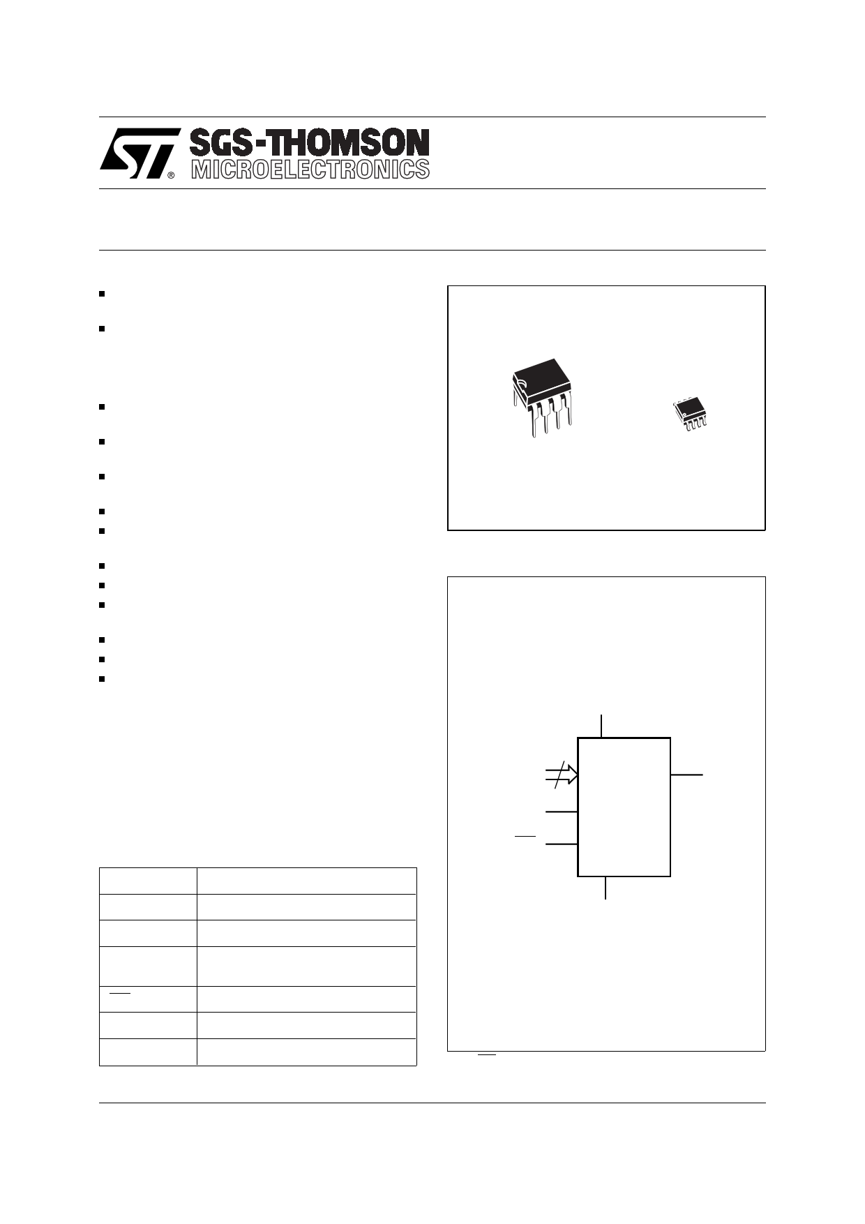
8
1
PSDIP8 (B)
0.25mm Frame
8
1
SO8 (M)
150mil Width
Figure 1. Logic Diagram
VCC
3
E0-E2
SCL
MODE/WC*
ST24x02
ST25x02
ST24C02R
SDA
VSS
AI00788D
Note: WC signal is only available for ST24/25W02 products.
November 1997
This is information on a product still in production but not recommended for new design
1/16
1 page 
ST24/25C02, ST24C02R, ST24/25W02
Table 5. Input Parameters (1) (TA = 25 °C, f = 100 kHz )
Symbol
Parameter
Test Condition
CIN Input Capacitance (SDA)
CIN
ZWCL
ZWCH
Input Capacitance (other pins)
WC Input Impedance (ST24/25W02)
WC Input Impedance (ST24/25W02)
VIN ≤ 0.3 VCC
VIN ≥ 0.7 VCC
tLP
Low-pass filter input time constant
(SDA and SCL)
Note: 1. Sampled only, not 100% tested.
Min Max Unit
8 pF
6 pF
5 20 kΩ
500 kΩ
100 ns
Table 6. DC Characteristics
(TA = 0 to 70°C, –20 to 85°C or –40 to 85°C; VCC = 3V to 5.5V, 2.5V to 5.5V or 1.8V to 5.5V)
Symbol
Parameter
Test Condition
Min Max
ILI Input Leakage Current
ILO Output Leakage Current
0V ≤ VIN ≤ VCC
0V ≤ VOUT ≤ VCC
SDA in Hi-Z
±2
±2
Supply Current (ST24 series)
ICC
Supply Current (ST25 series)
ICC1
Supply Current (Standby)
(ST24 series)
ICC2
Supply Current (Standby)
(ST25 series)
ICC3
Supply Current (Standby)
(ST24C02R)
ICC4
Supply Current (Standby)
(ST24C02R)
VIL Input Low Voltage (SCL, SDA)
VIH Input High Voltage (SCL, SDA)
VIL
Input Low Voltage
(E0-E2, MODE, WC)
VCC = 5V, fC = 100kHz
(Rise/Fall time < 10ns)
VCC = 2.5V, fC = 100kHz
VIN = VSS or VCC,
VCC = 5V
VIN = VSS or VCC,
VCC = 5V, fC = 100kHz
VIN = VSS or VCC,
VCC = 2.5V
VIN = VSS or VCC,
VCC = 2.5V, fC = 100kHz
VIN = VSS or VCC,
VCC = 3.6V
VIN = VSS or VCC,
VCC = 3.6V, fC = 100kHz
VIN = VSS or VCC,
VCC = 1.8V
VIN = VSS or VCC,
VCC = 1.8V, fC = 100kHz
–0.3
0.7 VCC
–0.3
2
1
100
300
5
50
20
60
10
20
0.3 VCC
VCC + 1
0.5
VIH
Input High Voltage
(E0-E2, MODE, WC)
VCC – 0.5 VCC + 1
Output Low Voltage (ST24 series)
IOL = 3mA, VCC = 5V
VOL Output Low Voltage (ST25 series) IOL = 2.1mA, VCC = 2.5V
Output Low Voltage
(ST24C02R)
IOL = 1mA, VCC = 1.8V
0.4
0.4
0.3
Unit
µA
µA
mA
mA
µA
µA
µA
µA
µA
µA
µA
µA
V
V
V
V
V
V
V
5/16
5 Page 
ST24/25C02, ST24C02R, ST24/25W02
Figure 9. Write Modes Sequence with Write Control = 1 (ST24/25W02)
WC
BYTE WRITE
WC
PAGE WRITE
WC (cont'd)
PAGE WRITE
(cont'd)
ACK
ACK
ACK
DEV SEL
BYTE ADDR
DATA IN
R/W
ACK
ACK
ACK
DEV SEL
BYTE ADDR DATA IN 1
DATA IN 2
R/W
ACK
ACK
DATA IN N
AI01101B
Sequential Read. This mode can be initiated with
either a Current Address Read or a Random Ad-
dress Read. However, in this case the master
DOES acknowledge the data byte output and the
memory continues to output the next byte in se-
quence. To terminate the stream of bytes, the
master must NOT acknowledge the last byte out-
put, but MUST generate a STOP condition. The
output data is from consecutive byte addresses,
with the internal byte address counter automat-
ically incremented after each byte output. After a
count of the last memory address, the address
counter will ’roll- over’ and the memory will continue
to output data.
Acknowledge in Read Mode. In all read modes
the ST24/25x02 wait for an acknowledge during the
9th bit time. If the master does not pull the SDA line
low during this time, the ST24/25x02 terminate the
data transfer and switches to a standby state.
11/16
11 Page | ||
| Páginas | Total 16 Páginas | |
| PDF Descargar | [ Datasheet ST24C02.PDF ] | |
Hoja de datos destacado
| Número de pieza | Descripción | Fabricantes |
| ST24C01 | SERIAL 1K 128 x 8 EEPROM | ST Microelectronics |
| ST24C01 | (ST2xxx) SERIAL 1K 128 x 8 EEPROM | ST Microelectronics |
| ST24C01R | (ST2xxx) SERIAL 1K 128 x 8 EEPROM | ST Microelectronics |
| ST24C02 | SERIAL 2K (256 x 8) EEPROM | ST Microelectronics |
| Número de pieza | Descripción | Fabricantes |
| SLA6805M | High Voltage 3 phase Motor Driver IC. |
Sanken |
| SDC1742 | 12- and 14-Bit Hybrid Synchro / Resolver-to-Digital Converters. |
Analog Devices |
|
DataSheet.es es una pagina web que funciona como un repositorio de manuales o hoja de datos de muchos de los productos más populares, |
| DataSheet.es | 2020 | Privacy Policy | Contacto | Buscar |