|
|
|
PDF 74LVX16373 Data sheet ( Hoja de datos )
| Número de pieza | 74LVX16373 | |
| Descripción | LOW VOLTAGE CMOS 16-BIT D-TYPE LATCH (3-STATE) WITH 5V TOLERANT INPUTS | |
| Fabricantes | ST Microelectronics | |
| Logotipo | ||
Hay una vista previa y un enlace de descarga de 74LVX16373 (archivo pdf) en la parte inferior de esta página. Total 10 Páginas | ||
|
No Preview Available !
74LVX16373
LOW VOLTAGE CMOS 16-BIT D-TYPE LATCH (3-STATE)
WITH 5V TOLERANT INPUTS
s HIGH SPEED :
tPD = 5.4 ns (MAX.) at VCC = 3V
s 5V TOLERANT INPUTS
s POWER DOWN PROTECTION ON INPUTS
s INPUT VOLTAGE LEVEL:
VIL = 0.8V, VIH = 2V at VCC =3V
s LOW POWER DISSIPATION:
ICC = 4 µA (MAX.) at TA=25°C
s LOW NOISE:
VOLP = 0.3V (TYP.) at VCC =3.3V
s SYMMETRICAL OUTPUT IMPEDANCE:
|IOH| = IOL = 4 mA (MIN) at VCC =3V
s BALANCED PROPAGATION DELAYS:
tPLH ≅ tPHL
s OPERATING VOLTAGE RANGE:
VCC(OPR) = 2V to 3.6V (1.2V Data Retention)
s PIN AND FUNCTION COMPATIBLE WITH
74 SERIES 16373
s IMPROVED LATCH-UP IMMUNITY
DESCRIPTION
The 74LVX16373 is a low voltage CMOS 16 BIT
D-TYPE LATCH with 3 STATE OUTPUTS NON
INVERTING fabricated with sub-micron silicon
gate and double-layer metal wiring C2MOS
technology. It is ideal for low power, battery
operated and low noise 3.3V applications.
These 16 bit D-TYPE latches are byte controlled
by two latch enable inputs (nLE) and two output
enable inputs(OE).
While the nLE input is held at a high level, the nQ
outputs will follow the data input precisely.
When the nLE is taken LOW, the nQ outputs will
be latched precisely at the logic level of D input
data.
While the (nOE) input is low, the nQ outputs will be
in a normal logic state (high or low logic level) and
while high level the outputs will be in a high imped-
ance state.
Power down protection is provided on all inputs
and 0 to 7V can be accepted on inputs with no
regard to the supply voltage.
This device can be used to interface 5V to 3V. It
combines high speed performance with the true
CMOS low power consumption.
All inputs and outputs are equipped with protec-
tion circuits against static discharge, giving them
2KV ESD immunity and transient excess voltage.
February 2003
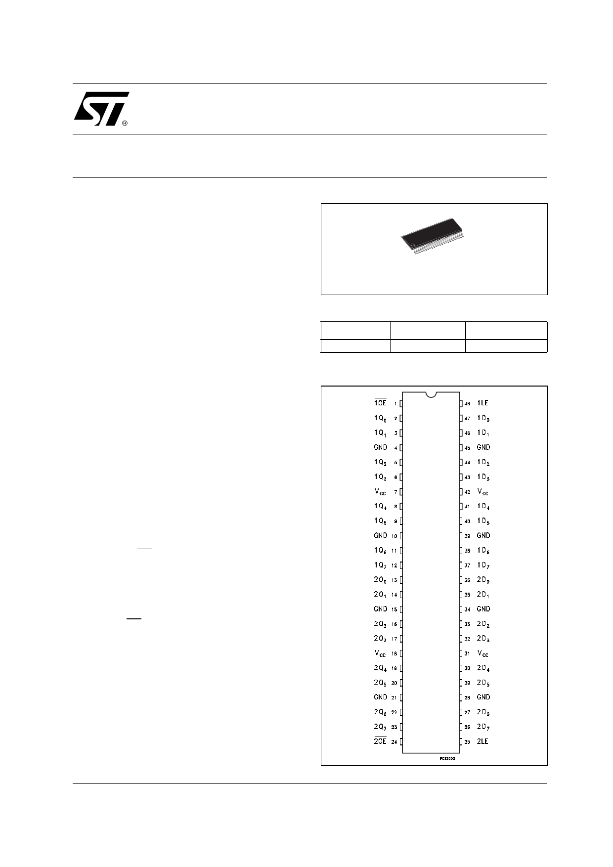
TSSOP
ORDER CODES
PACKAGE
TSSOP
TUBE
PIN CONNECTION
T&R
74LVX16373TTR
1/10
1 page 
74LVX16373
AC ELECTRICAL CHARACTERISTICS (Input tr = tf = 3ns)
Test Condition
Value
Symbol
Parameter
VCC CL
(V) (pF)
TA = 25°C
-40 to 85°C -55 to 125°C Unit
Min. Typ. Max. Min. Max. Min. Max.
tPLH Propagation Delay 2.7 15
tPHL Time
LE to Qn
2.7 50
3.3(*) 15
7 14 1 16 1 16
9 15.5 1 17 1 17
ns
5.5 13 1 15 1 15
3.3(*) 50
7 14.5 1 16.5 1 16.5
tPLH Propagation Delay 2.7 15
tPHL Time
Dn to Qn
2.7 50
3.3(*) 15
8 14 1 16 1 16
9.5 15 1 17 1 17
ns
5.4 13 1 15 1 15
3.3(*) 50
7.5 14 1 16 1 16.5
tPZL
tPZH
Output Enable
Time
2.7
2.7
3.3(*)
15
50
15
7 14.9 1 16 1 16
9.5 16 1 17 1 17
5.2 13 1 15 1 15 ns
3.3(*) 50
7.6 14.9 1 16 1 16
tPLZ
tPHZ
Output Disable
Time
2.7 50
3.3(*) 50
9 17 1 18 1 18
ns
7.7 15.5 1 17 1 17
tW
LE pulse Width,
HIGH
2.7 50
3.3(*) 50
6
5
66
ns
55
tS
Setup Time Dn to
LE HIGH or LOW
2.7 50
3.3(*) 50
4.5
4
4.5 4.5
ns
44
th
Hold Time Dn to LE 2.7 50
HIGH or LOW
3.3(*) 50
1.5
1
1.5 1.5
ns
11
tOSLH
tOSHL
Output to Output
Skew Time (note
1,2)
2.7 50
3.3(*) 50
0.5 1.0 1.5 1.5
ns
0.5 1.0 1.5 1.5
1) Skew is defined as the absolute value of the difference between the actual propagation delay for any two outputs of the same device switch-
ing in the same direction, either HIGH or LOW
2) Parameter guaranteed by design
(*) Voltage range is 3.3V ± 0.3V
CAPACITIVE CHARACTERISTICS
Test Condition
Value
Symbol
Parameter
VCC
(V)
TA = 25°C
-40 to 85°C -55 to 125°C Unit
Min. Typ. Max. Min. Max. Min. Max.
CIN Input Capacitance
2.5 10 10 10 pF
COUT Output
Capacitance
4 pF
CPD Power Dissipation
Capacitance
3.0
(note 1)
fIN = 10MHz
17
pF
1) CPD is defined as the value of the IC’s internal equivalent capacitance which is calculated from the operating current consumption without
load. (Refer to Test Circuit). Average operating current can be obtained by the following equation. ICC(opr) = CPD x VCC x fIN + ICC/n (per circuit)
5/10
5 Page | ||
| Páginas | Total 10 Páginas | |
| PDF Descargar | [ Datasheet 74LVX16373.PDF ] | |
Hoja de datos destacado
| Número de pieza | Descripción | Fabricantes |
| 74LVX16373 | LOW VOLTAGE CMOS 16-BIT D-TYPE LATCH (3-STATE) WITH 5V TOLERANT INPUTS | ST Microelectronics |
| Número de pieza | Descripción | Fabricantes |
| SLA6805M | High Voltage 3 phase Motor Driver IC. |
Sanken |
| SDC1742 | 12- and 14-Bit Hybrid Synchro / Resolver-to-Digital Converters. |
Analog Devices |
|
DataSheet.es es una pagina web que funciona como un repositorio de manuales o hoja de datos de muchos de los productos más populares, |
| DataSheet.es | 2020 | Privacy Policy | Contacto | Buscar |