|
|
PDF ID80C88 Data sheet ( Hoja de datos )
| Número de pieza | ID80C88 | |
| Descripción | CMOS 8/16-Bit Microprocessor | |
| Fabricantes | Intersil Corporation | |
| Logotipo |  |
|
Hay una vista previa y un enlace de descarga de ID80C88 (archivo pdf) en la parte inferior de esta página. Total 30 Páginas | ||
|
No Preview Available !
80C88
March 1997
CMOS 8/16-Bit Microprocessor
[ /Title
(80C88
)
/Sub-
ject
(CMO
S 8/16-
Bit
Micro-
proces-
sor)
/Autho
r ()
/Key-
words
(Inter-
sil
Corpo-
ration,
8/16
Bit uP,
micro-
proces-
sor, 8
bit, 16
bit, 8-
bit, 16-
bit,
8088,
PC)
/Cre-
ator ()
Features
Description
• Compatible with NMOS 8088
• Direct Software Compatibility with 80C86, 8086, 8088
• 8-Bit Data Bus Interface; 16-Bit Internal Architecture
• Completely Static CMOS Design
- DC . . . . . . . . . . . . . . . . . . . . . . . . . . . . . 5MHz (80C88)
- DC . . . . . . . . . . . . . . . . . . . . . . . . . . . .8MHz (80C88-2)
• Low Power Operation
- ICCSB . . . . . . . . . . . . . . . . . . . . . . . . 500µA Maximum
- ICCOP . . . . . . . . . . . . . . . . . . . . 10mA/MHz Maximum
• 1 Megabyte of Direct Memory Addressing Capability
The Intersil 80C88 high performance 8/16-bit CMOS CPU is
manufactured using a self-aligned silicon gate CMOS pro-
cess (Scaled SAJI IV). Two modes of operation, MINimum
for small systems and MAXimum for larger applications such
as multiprocessing, allow user configuration to achieve the
highest performance level.
Full TTL compatibility (with the exception of CLOCK) and
industry-standard operation allow use of existing NMOS
8088 hardware and Intersil CMOS peripherals.
Complete software compatibility with the 80C86, 8086, and
8088 microprocessors allows use of existing software in new
designs.
• 24 Operand Addressing Modes
• Bit, Byte, Word, and Block Move Operations
• 8-Bit and 16-Bit Signed/Unsigned Arithmetic
• Bus-Hold Circuitry Eliminates Pull-up Resistors
• Wide Operating Temperature Ranges
- C80C88 . . . . . . . . . . . . . . . . . . . . . . . . . 0oC to + 70oC
- I80C88 . . . . . . . . . . . . . . . . . . . . . . . . . -40oC to +85oC
- M80C88 . . . . . . . . . . . . . . . . . . . . . . . -55oC to +125oC
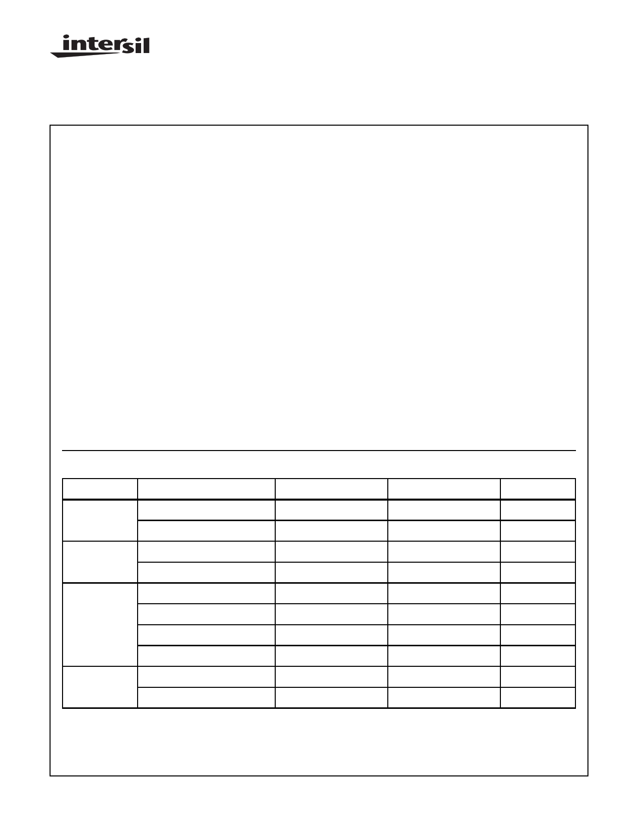
Ordering Information
PACKAGE
Plastic DIP
PLCC
CERDIP
SMD#
LCC
SMD#
TEMPERATURE RANGE
0oC to +70oC
-40oC to +85oC
0oC to +70oC
-40oC to +85oC
0oC to +70oC
-40oC to +85oC
-55oC to +125oC
-55oC to +125oC
-55oC to +125oC
-55oC to +125oC
5MHz
CP80C88
IP80C88
CS80C88
lS80C88
CD80C88
ID80C88
MD80C88/B
5962-8601601QA
MR80C88/B
5962-8601601XA
8MHz
CP80C88-2
IP80C88-2
CS80C88-2
IS80C88-2
CD80C88-2
ID80C88-2
MD80C88-2/B
-
MR80C88-2/B
-
PKG. NO.
E40.6
E40.6
N44.65
N44.65
F40.6
F40.6
F40.6
F40.6
J44.A
J44.A
CAUTION: These devices are sensitive to electrostatic discharge; follow proper IC Handling Procedures.
http://www.intersil.com or 407-727-9207 | Copyright © Intersil Corporation 1999
3-1
File Number 2949.1
1 page 
80C88
Pin Description (Continued)
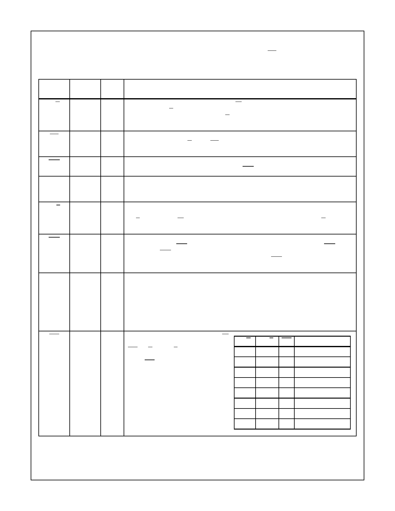
The following pin function descriptions are for 80C88 system in minimum mode (i.e., MN/MX = VCC). Only the pin functions
which are unique to the minimum mode are described; all other pin functions are as described above.
MINIMUM MODE SYSTEM
PIN
SYMBOL NUMBER TYPE
DESCRIPTION
IO/M 28 O STATUS LINE: is an inverted maximum mode S2. It is used to distinguish a memory access from
an I/O access. IO/M becomes valid in the T4 preceding a bus cycle and remains valid until the final
T4 of the cycle (I/O = HIGH, M = LOW). IO/M is held to a high impedance logic one during local bus
“hold acknowledge”.
WR 29 O Write: strobe indicates that the processor is performing a write memory or write I/O cycle, depend-
ing on the state of the IO/M signal. WR is active for T2, T3, and Tw of any write cycle. It is active
LOW, and is held to high impedance logic one during local bus “hold acknowledge”.
INTA 24 O INTA: is used as a read strobe for interrupt acknowledge cycles. It is active LOW during T2, T3 and
Tw of each interrupt acknowledge cycle. Note that INTA is never floated.
ALE 25 O ADDRESS LATCH ENABLE: is provided by the processor to latch the address into the
82C82/82C83 address latch. It is a HIGH pulse active during clock low of T1 of any bus cycle. Note
that ALE is never floated.
DT/R 27 O DATA TRANSMIT/RECEIVE: is needed in a minimum system that desires to use an 82C86/82C87
data bus transceiver. It is used to control the direction of data flow through the transceiver. Logically,
DT/R is equivalent to S1 in the maximum mode, and its timing is the same as for IO/M (T = HIGH,
R = LOW). This signal is held to a high impedance logic one during local bus “hold acknowledge”.
DEN 26 O DATA ENABLE: is provided as an output enable for the 82C86/82C87 in a minimum system which
uses the transceiver. DEN is active LOW during each memory and I/O access, and for INTA cycles.
For a read or INTA cycle, it is active from the middle of T2 until the middle of T4, while for a write
cycle, it is active from the beginning of T2 until the middle of T4. DEN is held to high impedance logic
one during local bus “hold acknowledge”.
HOLD,
HLDA
31
30
I HOLD: indicates that another master is requesting a local bus “hold”. To be acknowledged, HOLD
O must be active HIGH. The processor receiving the “hold” request will issue HLDA (HIGH) as an
acknowledgment, in the middle of a T4 or T1 clock cycle. Simultaneous with the issuance of HLDA
the processor will float the local bus and control lines. After HOLD is detected as being LOW, the
processor lowers HLDA, and when the processor needs to run another cycle, it will again drive the
local bus and control lines.
Hold is not an asynchronous input. External synchronization should be provided if the system cannot
otherwise guarantee the set up time.
SS0 34 O STATUS LINE: is logically equivalent to S0
in the maximum mode. The combination of IO/M DT/R SS0 CHARACTERISTICS
SS0, IO/M and DT/R allows the system to
completely decode the current bus cycle
status. SS0 is held to high impedance logic
1
1
0 0 Interrupt Acknowledge
0 1 Read I/O Port
one during local bus “hold acknowledge”.
1 1 0 Write I/O Port
1 1 1 Halt
0 0 0 Code Access
0 0 1 Read Memory
0 1 0 Write Memory
0 1 1 Passive
3-5
5 Page 
80C88
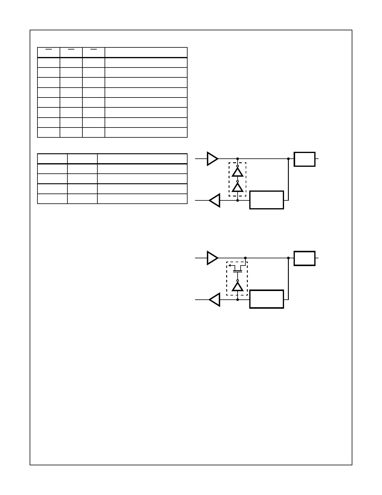
TABLE 7.
S2 S1 S0
CHARACTERISTICS
0 0 0 Interrupt Acknowledge
0 0 1 Read I/O
0 1 0 Write I/O
0 1 1 Halt
1 0 0 Instruction Fetch
1 0 1 Read Data from Memory
1 1 0 Write Data to Memory
1 1 1 Passive (No Bus Cycle)
TABLE 8.
S4 S3
CHARACTERISTICS
0 0 Alternate Data (Extra Segment)
0 1 Stack
1 0 Code or None
1 1 Data
I/O Addressing
In the 80C88, I/O operations can address up to a maximum
of 64K I/O registers. The I/O address appears in the same
format as the memory address on bus lines A15-A0. The
address lines A19-A16 are zero in I/O operations. The vari-
able I/O instructions, which use register DX as a pointer,
have full address capability, while the direct I/O instructions
directly address one or two of the 256 I/O byte locations in
page 0 of the I/O address space. I/O ports are addressed in
the same manner as memory locations.
Designers familiar with the 8085 or upgrading an 8085
design should note that the 8085 addresses I/O with an 8-bit
address on both halves of the 16-bit address bus. The
80C88 uses a full 16-bit address on its lower 16 address
lines.
Bus Hold Circuitry
To avoid high current conditions caused by floating inputs to
CMOS devices and to eliminate the need for pull-up/down
resistors, “bus-hold” circuitry has been used on 80C88 pins
2-16, 26-32 and 34-39 (see Figure 6A and 6B). These
circuits maintain a valid logic state if no driving source is
present (i.e., an unconnected pin or a driving source which
goes to a high impedance state).
To override the “bus hold” circuits, an external driver must be
capable of supplying 400µA minimum sink or source current
at valid input voltage levels. Since this “bus hold” circuitry is
active and not a “resistive” type element, the associated
power supply current is negligible. Power dissipation is sig-
nificantly reduced when compared to the use of passive pull-
up resistors.
OUTPUT
DRIVER
BOND
PAD
EXTERNAL
PIN
INPUT
BUFFER
INPUT
PROTECTION
CIRCUITRY
FIGURE 19A. BUS HOLD CIRCUITRY PIN 2-16, 35-39
OUTPUT VCC
DRIVER
P
BOND
PAD
EXTERNAL
PIN
INPUT
BUFFER
INPUT
PROTECTION
CIRCUITRY
FIGURE 19B. BUS HOLD CIRCUITRY PIN 26-32, 34
External Interface
Processor Reset and Initialization
Processor initialization or start up is accomplished with
activation (HIGH) of the RESET pin. The 80C88 RESET is
required to be HIGH for greater than four clock cycles. The
80C88 will terminate operations on the high-going edge of
RESET and will remain dormant as long as RESET is HIGH.
The low-going transition of RESET triggers an internal reset
sequence for approximately 7 clock cycles. After this interval
the 80C88 operates normally, beginning with the instruction
in absolute location FFFFOH (see Figure 2). The RESET
input is internally synchronized to the processor clock. At
initialization, the HIGH to LOW transition of RESET must
occur no sooner than 50µs after power up, to allow complete
initialization of the 80C88.
NMI will not be recognized if asserted prior to the second
CLK cycle following the end of RESET.
Interrupt Operations
Interrupt operations fall into two classes: software or
hardware initiated. The software initiated interrupts and
software aspects of hardware interrupts are specified in the
instruction set description. Hardware interrupts can be
classified as nonmaskable or maskable.
Interrupts result in a transfer of control to a new program
location. A 256 element table containing address pointers to
the interrupt service program locations resides in absolute
locations 0 through 3FFH (see Figure 2), which are reserved
for this purpose. Each element in the table is 4 bytes in size
and corresponds to an interrupt “type”. An interrupting
device supplies an 8-bit type number, during the interrupt
acknowledge sequence, which is used to vector through the
appropriate element to the new interrupt service program
location.
3-11
11 Page | ||
| Páginas | Total 30 Páginas | |
| PDF Descargar | [ Datasheet ID80C88.PDF ] | |
Hoja de datos destacado
| Número de pieza | Descripción | Fabricantes |
| ID80C86 | CMOS 16-Bit Microprocessor | Intersil Corporation |
| ID80C88 | CMOS 8/16-Bit Microprocessor | Intersil Corporation |
| Número de pieza | Descripción | Fabricantes |
| SLA6805M | High Voltage 3 phase Motor Driver IC. |
Sanken |
| SDC1742 | 12- and 14-Bit Hybrid Synchro / Resolver-to-Digital Converters. |
Analog Devices |
|
DataSheet.es es una pagina web que funciona como un repositorio de manuales o hoja de datos de muchos de los productos más populares, |
| DataSheet.es | 2020 | Privacy Policy | Contacto | Buscar |
