|
|
|
PDF AD5259 Data sheet ( Hoja de datos )
| Número de pieza | AD5259 | |
| Descripción | 256-Position Digital Potentiometer | |
| Fabricantes | Analog Devices | |
| Logotipo | ||
Hay una vista previa y un enlace de descarga de AD5259 (archivo pdf) en la parte inferior de esta página. Total 24 Páginas | ||
|
No Preview Available !
Nonvolatile, I2C-Compatible
256-Position, Digital Potentiometer
AD5259
FEATURES
Nonvolatile memory maintains wiper settings
256-position
Thin LFCSP-10 (3 mm x 3 mm x 0.8 mm) package
Compact MSOP-10 (3 mm × 4.9 mm x 1.1mm) package
I2C®-compatible interface
VLOGIC pin provides increased interface flexibility
End-to-end resistance 5 kΩ, 10 kΩ, 50 kΩ, 100 kΩ
Resistance tolerance stored in EEPROM (0.1% accuracy)
Power-on EEPROM refresh time < 1ms
Software write protect command
Address Decode Pin AD0 and Pin AD1 allow
4 packages per bus
100-year typical data retention at 55°C
Wide operating temperature −40°C to +85°C
3 V to 5 V single supply
APPLICATIONS
LCD panel VCOM adjustment
LCD panel brightness and contrast control
Mechanical potentiometer replacement in new designs
Programmable power supplies
RF amplifier biasing
Automotive electronics adjustment
Gain control and offset adjustment
Fiber to the home systems
Electronics level settings
GENERAL DESCRIPTION
The AD5259 provides a compact, nonvolatile LFCSP-10
(3 mm × 3 mm) or MSOP-10 (3 mm × 4.9 mm) packaged
solution for 256-position adjustment applications. These
devices perform the same electronic adjustment function
as mechanical potentiometers1 or variable resistors, but
with enhanced resolution and solid-state reliability.
The wiper settings are controllable through an I2C-compatible
digital interface that is also used to read back the wiper register
and EEPROM content. Resistor tolerance is also stored within
EEPROM, providing an end-to-end tolerance accuracy of 0.1%.
A separate VLOGIC pin delivers increased interface flexibility. For
users who need multiple parts on one bus, Address Bit AD0 and
Address Bit AD1 allow up to four devices on the same bus.
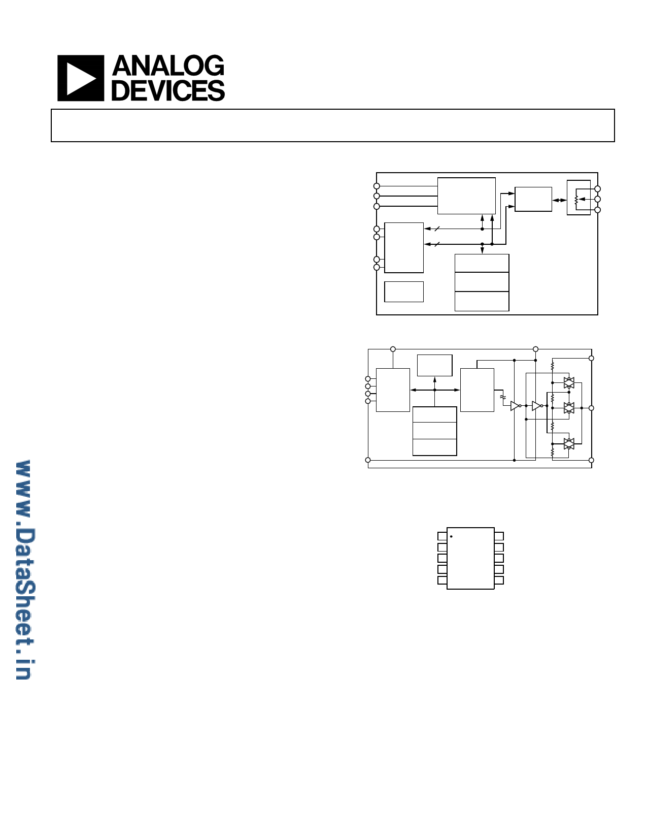
FUNCTIONAL BLOCK DIAGRAMS
VDD
VLOGIC
GND
SCL
SDA
AD0
AD1
RDAC
EEPROM
RDAC
REGISTER
RDAC
I2C
SERIAL
INTERFACE
POWER-
ON RESET
8 DATA
8 CONTROL
COMMAND
DECODE LOGIC
ADDRESS
DECODE LOGIC
CONTROL LOGIC
AD5259
A
W
B
VLOGIC
Figure 1. Block Diagram
VDD
SCL
SDA
AD0
AD1
GND
EEPROM
I2C
SERIAL
INTERFACE
COMMAND
DECODE LOGIC
ADDRESS
DECODE LOGIC
CONTROL
LOGIC
RDAC
REGISTER
AND
LEVEL
SHIFTER
Figure 2. Block Diagram Showing Level Shifters
A
W
B
CONNECTION DIAGRAM
W1
10 A
AD0 2 AD5259 9 B
AD1 3 TOP VIEW 8 VDD
SDA 4 (Not to Scale) 7 GND
SCL 5
6 VLOGIC
Figure 3. Pinout
1 The terms digital potentiometer, VR (variable resistor), and RDAC are used
interchangeably.
Rev. A
Information furnished by Analog Devices is believed to be accurate and reliable.
However, no responsibility is assumed by Analog Devices for its use, nor for any
infringements of patents or other rights of third parties that may result from its use.
Specifications subject to change without notice. No license is granted by implication
or otherwise under any patent or patent rights of Analog Devices. Trademarks and
registered trademarks are the property of their respective owners.
One Technology Way, P.O. Box 9106, Norwood, MA 02062-9106, U.S.A.
Tel: 781.329.4700
www.analog.com
Fax: 781.461.3113 © 2005 Analog Devices, Inc. All rights reserved.
1 page 
AD5259
TIMING CHARACTERISTICS
VDD = VLOGIC = 5 V ± 10% or 3 V ± 10%; VA = VDD; VBB = 0 V; −40°C < TA < +85°C, unless otherwise noted.
Table 2.
Parameter
Symbol
Conditions
Min Typ Max Unit
I2C INTERFACE TIMING
CHARACTERISTICS1
SCL Clock Frequency
fSCL
0 400 kHz
tBUF Bus Free Time Between Stop
and Start
t1
1.3 μs
tHD;STA Hold Time (Repeated Start)
t2
After this period, the first clock pulse is
generated.
0.6
μs
tLOW Low Period of SCL Clock
t3
1.3 μs
tHIGH High Period of SCL Clock
t4
0.6 μs
tSU;STA Setup Time for Repeated
Start Condition
t5
0.6 μs
tHD;DAT Data Hold Time
t6
0 0.9 μs
tSU;DAT Data Setup Time
t7
100 ns
tF Fall Time of Both SDA and
SCL Signals
t8
300 ns
tR Rise Time of Both SDA and
SCL Signals
t9
300 ns
tSU;STO Setup Time for Stop Condition t10
0.6 μs
EEPROM Data Storing Time
tEEMEM_STORE
26 ms
EEPROM Data Restoring Time at
tEEMEM_RESTORE1 VDD rise time dependent. Measure without
300
μs
Power On2
decoupling capacitors at VDD and GND.
EEPROM Data Restoring Time upon
Restore Command2
tEEMEM_RESTORE2 VDD = 5 V.
300 μs
EEPROM Data Rewritable Time3
tEEMEM_REWRITE
540 μs
FLASH/EE MEMORY RELIABILITY
Endurance4
100 700
kCycles
Data Retention5
100 Years
1 Standard I2C mode operation guaranteed by design.
2 During power-up, the output is momentarily preset to midscale before restoring EEPROM content.
3 Delay time after power-on PRESET prior to writing new EEPROM data.
4 Endurance is qualified to 100,000 cycles per JEDEC Std. 22 method A117, and is measured at –40°C, +25°C, and +85°C; typical endurance at +25°C is 700,000 cycles.
5 Retention lifetime equivalent at junction temperature (TJ) = 55°C per JEDEC Std. 22, Method A117. Retention lifetime based on an activation energy of 0.6 eV derates
with junction temperature.
SCL
t2
SDA
t1
PS
t8 t6 t9
t3
t8 t9
t4
t7
t2
t5
S
Figure 4. I2C Interface Timing Diagram
t10
P
Rev. A | Page 5 of 24
5 Page 
0
80H
–6
40H
–12
–18 20H
–24 10H
08H
–30
04H
–36
02H
–42
01H
–48
–54
–60
1k
10k 100k
FREQUENCY (Hz)
Figure 24. Gain vs. Frequency vs. Code, RAB = 50 kΩ
1M
0
80H
–6
40H
–12
–18 20H
–24 10H
08H
–30
–36 04H
02H
–42
01H
–48
–54
–60
1k
10k 100k
FREQUENCY (Hz)
Figure 25. Gain vs. Frequency vs. Code, RAB = 100 kΩ
1M
0
–6
–12
100kΩ
–18 80kHz
50kΩ
–24 160kHz
10kΩ
–30 800kHz
5kΩ
–36 2MHz
–42
–48
–54
–60
1k
10k 100k
FREQUENCY (Hz)
1M
Figure 26. −3 dB Bandwidth @ Code = 0×80
10M
AD5259
10k
VDD = VLOGIC = 5V
1k
VDD = VLOGIC = 3V
100
10
01234
VIH (V)
Figure 27. Logic Supply Current vs. Input Voltage
5
80
CODE = MIDSCALE, VA = VLOGIC, VB = 0V
PSRR @ VLOGIC = 5V DC ± 10% p-p AC
60
40
PSRR @ VLOGIC = 3V DC ± 10% p-p AC
20
0
100 1k 10k 100k
FREQUENCY (Hz)
Figure 28. PSRR vs. Frequency
1M
VW
1
SCL
2
400ns/DIV
Figure 29. Digital Feedthrough
Rev. A | Page 11 of 24
11 Page | ||
| Páginas | Total 24 Páginas | |
| PDF Descargar | [ Datasheet AD5259.PDF ] | |
Hoja de datos destacado
| Número de pieza | Descripción | Fabricantes |
| AD5251 | (AD5251 / AD5252) Dual 64-and 256-Position I2C Nonvolatile Memory Digital Potentiometers | Analog Devices |
| AD5252 | (AD5251 / AD5252) Dual 64-and 256-Position I2C Nonvolatile Memory Digital Potentiometers | Analog Devices |
| AD5253 | Quad 64-/256-Position I2C Nonvolatile Memory Digital Potentiometers | Analog Devices |
| AD5254 | Quad 64-/256-Position I2C Nonvolatile Memory Digital Potentiometers | Analog Devices |
| Número de pieza | Descripción | Fabricantes |
| SLA6805M | High Voltage 3 phase Motor Driver IC. |
Sanken |
| SDC1742 | 12- and 14-Bit Hybrid Synchro / Resolver-to-Digital Converters. |
Analog Devices |
|
DataSheet.es es una pagina web que funciona como un repositorio de manuales o hoja de datos de muchos de los productos más populares, |
| DataSheet.es | 2020 | Privacy Policy | Contacto | Buscar |