|
|
PDF 44608P40 Data sheet ( Hoja de datos )
| Número de pieza | 44608P40 | |
| Descripción | MC44608 | |
| Fabricantes | ON Semiconductor | |
| Logotipo | ||
Hay una vista previa y un enlace de descarga de 44608P40 (archivo pdf) en la parte inferior de esta página. Total 16 Páginas | ||
|
No Preview Available !
www.DataSheet4U.com
MC44608
Few External Components
Reliable and Flexible
GreenLine ™ Very High Voltage
PWM Controller
The MC44608 is a high performance voltage mode controller
designed for off–line converters. This high voltage circuit that
integrates the start–up current source and the oscillator capacitor,
requires few external components while offering a high flexibility and
reliability.
The device also features a very high efficiency stand–by
management consisting of an effective Pulsed Mode operation. This
technique enables the reduction of the stand–by power consumption to
approximately 1W while delivering 300mW in a 150W SMPS.
• Integrated Start–Up Current Source
• Lossless Off–Line Start–Up
• Direct Off–Line Operation
• Fast Start–Up
General Features
• Flexibility
• Duty Cycle Control
• Undervoltage Lockout with Hysteresis
• On Chip Oscillator Switching Frequency 40, or 75kHz
• Secondary Control with Few External Components
Protections
• Maximum Duty Cycle Limitation
• Cycle by Cycle Current Limitation
• Demagnetization (Zero Current Detection) Protection
• “Over VCC Protection” Against Open Loop
• Programmable Low Inertia Over Voltage Protection Against Open Loop
• Internal Thermal Protection
GreenLine™ Controller
• Pulsed Mode Techniques for a Very High Efficiency Low Power
Mode
• Lossless Startup
• Low dV/dT for Low EMI Radiations
http://onsemi.com
8
1
DIP–8
P SUFFIX
CASE 626
PIN CONNECTIONS AND
MARKING DIAGRAM
Demag 1
Isense 2
Control Input 3
Gnd 4
8 Vi
7
6 Vcc
5 Driver
AWL = Manufacturing Code
YYWW = Date Code
(Top View)
ORDERING INFORMATION
Device
MC44608P40
Switching Package Shipping
Frequency
40kHz
Plastic 50 / Rail
DIP–8
MC44608P75
75kHz
Plastic 50 / Rail
DIP–8
© Semiconductor Components Industries, LLC, 1999
January, 2000 – Rev. 2
1
Publication Order Number:
MC44608/D
1 page 
www.DataSheet4U.com
MC44608
PIN FUNCTION DESCRIPTION
Pin Name
Description
1
Demag
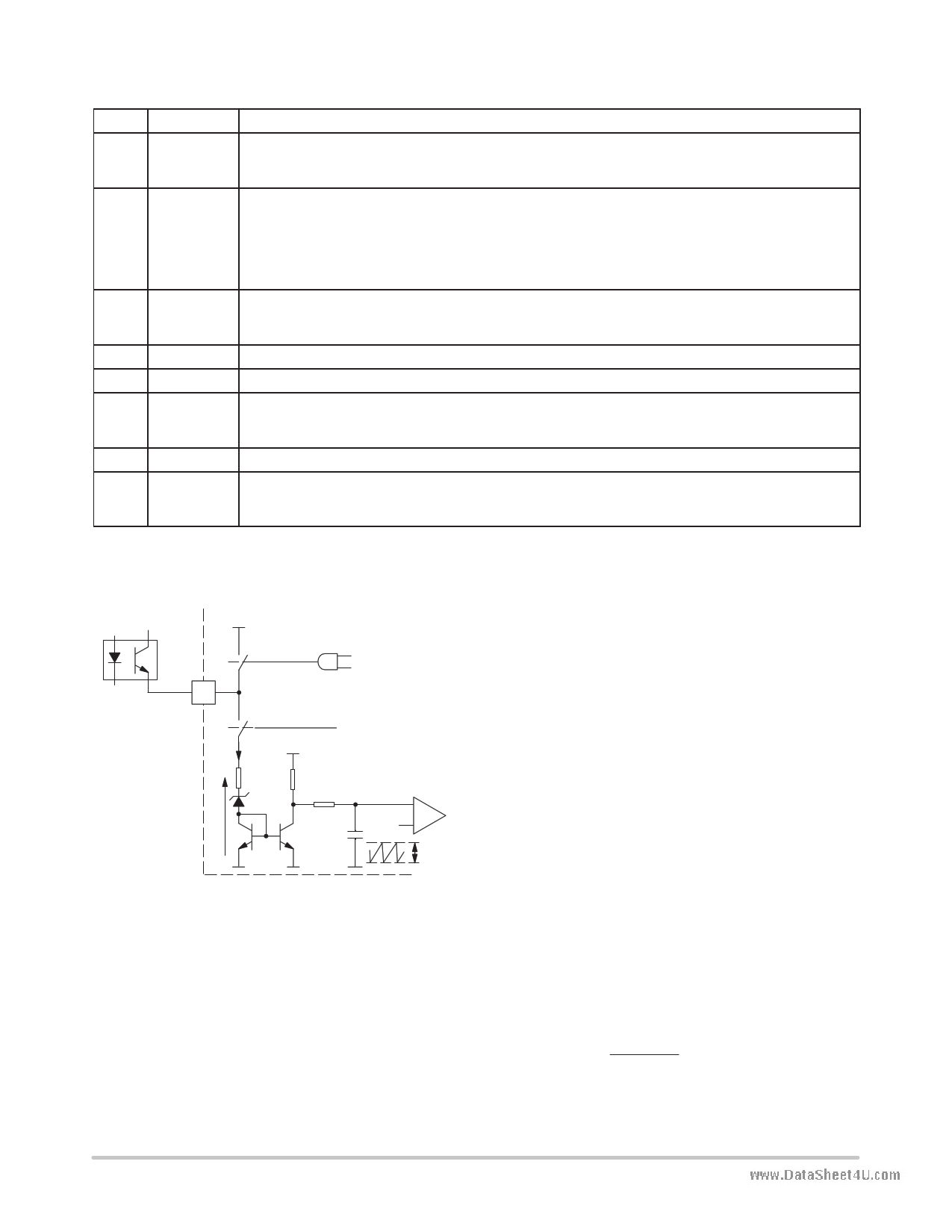
The Demag pin offers 3 different functions: Zero voltage crossing detection (50mV), 24µA current detection
and 120µA current detection. The 24µA level is used to detect the secondary reconfiguration status and the
120µA level to detect an Over Voltage status called Quick OVP.
2
Isense
The Current Sense pin senses the voltage developed on the series resistor inserted in the source of the
power MOSFET. When Isense reaches 1V, the Driver output (pin 5) is disabled. This is known as the Over
Current Protection function. A 200µA current source is flowing out of the pin 3 during the start–up phase and
during the switching phase in case of the Pulsed Mode of operation. A resistor can be inserted between the
sense resistor and the pin 3, thus a programmable peak current detection can be performed during the SMPS
stand–by mode.
3 Control Input A feedback current from the secondary side of the SMPS via the opto–coupler is injected into this pin. A
resistor can be connected between this pin and GND to allow the programming of the Burst duty cycle during
the Stand–by mode.
4
Ground
This pin is the ground of the primary side of the SMPS.
5
Driver
The current and slew rate capability of this pin are suited to drive Power MOSFETs.
6
VCC
This pin is the positive supply of the IC. The driver output gets disabled when the voltage becomes higher
than 15V and the operating range is between 6.6V and 13V. An intermediate voltage level of 10V creates a
disabling condition called Latched Off phase.
7 This pin is to provide isolation between the Vi pin 8 and the VCC pin 6.
8 Vi This pin can be directly connected to a 500V voltage source for start–up function of the IC. During the
Start–up phase a 9 mA current source is internally delivered to the VCC pin 6 allowing a rapid charge of the
VCC capacitor. As soon as the IC starts–up, this current source is disabled.
OPERATING DESCRIPTION
Regulation
V CC
V LP–stby
Control
Input
1
S3
3
0
&
Stand–by
Latched off Phase
10
S2
Vdd
Switching Phase
20 W
Regulation
Output
PWM
Comparator
5 V 4 kHz
Filter
1.6 V
Figure 1. Regulator
The switch S3 is closed in Stand–by mode during the
Latched Off Phase while the switch S2 remains open. (See
section PULSED MODE DUTY CYCLE CONTROL).
The resistor Rdpulsed (Rduty cycle burst) has no effect on
the regulation process. This resistor is used to determine the
burst duty cycle described in the chapter “Pulsed Duty Cycle
Control” on page 8.
PWM Latch
The MC44608 works in voltage mode. The on–time is
controlled by the PWM comparator that compares the
oscillator sawtooth with the regulation block output (refer to
the block diagram on page 2).
The PWM latch is initialized by the oscillator and is reset
by the PWM comparator or by the current sense comparator
in case of an over current. This configuration ensures that
only a single pulse appears at the circuit output during an
oscillator cycle.
The pin 3 senses the feedback current provided by the opto
coupler. During the switching phase the switch S2 is closed
and the shunt regulator is accessible by the pin 3. The shunt
regulator voltage is typically 5V. The dynamic resistance of
the shunt regulator represented by the zener diode is 20W.
The gain of the Control input is given on Figure 10 which
shows the duty cycle as a function of the current injected into
the pin 3.
A 4kHz filter network is inserted between the shunt
regulator and the PWM comparator to cancel the high
frequency residual noise.
Current Sense
The inductor current is converted to a positive voltage by
inserting a ground reference sense resistor RSense in series
with the power switch.
The maximum current sense threshold is fixed at 1V. The
peak current is given by the following equation:
+Ipkmax
1
Rsense(W
)
(A)
http://onsemi.com
5
5 Page 
www.DataSheet4U.com
MC44608
60
50
40
30
20
10
10
79.0
77.0
75.0
73.0
71.0
69.0
67.0
65.0
10
t_rise
t_fall
11 12 13 14
Pin6 VCC Voltage (V)
Figure 8. Output Switching Speed
15
–25° C
85° C
25° C
11 12 13 14
VCC Voltage (V)
Figure 9. Frequency Stability
15
5.08
5.07
5.06
5.05
5.04
5.03
5.02
5.01
5.00
4.99
4.98
0.5
85° C
–25° C
1
25° C
1.5 2
2.5
Current Injected in Pin 3 (mA)
Figure 11. Vpin3 During the Working Period
5.0
4.5
4.0 –25° C
3.5
25° C
3.0
2.5
85° C
2.0
1.5
–1.6 –1.4 –1.2 –1.0 –.08 –.06 –.04 –.02 0.0
Current Injected in Pin 3 (mA)
Figure 12. Vpin3 During the Latched Off Period
90
80
70
60
50 85° C
40
30
20
10
0
0.0 0.5
–25° C
25° C
1.0 1.5
Current Injected in Pin3 (mA)
2.0
Figure 10. Duty Cycle Control
4.80
4.60
4.40
4.20
4.00
3.80
3.60
3.40
3.20
3.00
2.5 10
–25° C
25° C
85° C
11 12 13 14
Pin6 VCC Voltage (V)
15
Figure 13. Device Consumption when Switching
http://onsemi.com
11
11 Page | ||
| Páginas | Total 16 Páginas | |
| PDF Descargar | [ Datasheet 44608P40.PDF ] | |
Hoja de datos destacado
| Número de pieza | Descripción | Fabricantes |
| 44608P40 | MC44608 | ON Semiconductor |
| Número de pieza | Descripción | Fabricantes |
| SLA6805M | High Voltage 3 phase Motor Driver IC. |
Sanken |
| SDC1742 | 12- and 14-Bit Hybrid Synchro / Resolver-to-Digital Converters. |
Analog Devices |
|
DataSheet.es es una pagina web que funciona como un repositorio de manuales o hoja de datos de muchos de los productos más populares, |
| DataSheet.es | 2020 | Privacy Policy | Contacto | Buscar |
