|
|
|
PDF V96BMC Data sheet ( Hoja de datos )
| Número de pieza | V96BMC | |
| Descripción | High Performance Burst DRAM Controller | |
| Fabricantes | V3 Semiconductor | |
| Logotipo | ||
Hay una vista previa y un enlace de descarga de V96BMC (archivo pdf) en la parte inferior de esta página. Total 14 Páginas | ||
|
No Preview Available !
.com V96BMC Rev. DHIGH PERFORMANCE BURST
DRAM CONTROLLER
t4U FOR i960Cx/Hx/Jx® PROCESSORS
ee• Pin/Software compatible with earlier V96BMC.
Sh• Direct interfaces to i960Cx/Hx/Jx processors.
ta• 3.3V DRAM interface support.
.Da• Near SRAM performance achieved with DRAM.
w • Supports up to 512Mb of DRAM.
w • Interleaved or non-interleaved operation.
w • Supports symmetric and non-symmetric arrays.
mThe V96BMC Revision D Burst DRAM Controller
ois an enhanced version of the previous V96BMC
.cwith improved timing and provides dedicated
Power and Ground rails to support the
increasingly popular 3.3V DRAM modules.
UTiming parameters are also improved over the
older versions of the device.
t4The V96BMC provides the DRAM access
eprotocols, buffer signals, data multiplexer
signals, and bus timing resources required to
ework with DRAM. By using the V96BMC, system
designers can replace tedious design work,
hexpensive FPGAs and valuable board space
with a single, high-performance, easily
Sconfigured device. The processor interface of the
taV96BMC implements the bus protocol of the
i960Cx/Hx/Jx. The pin naming convention has
been duplicated on the V96BMC; simply wire
alike-named pins together to create the interface.
.DThe V96BMC supports a total DRAM memory
subsystem size of 512Mbytes. The array may be
• Software-configured operational parameters.
• Integrated Page Cache Management.
• 2Kbyte burst transaction support.
• On chip memory address multiplexer/drivers.
• Two 24-bit timers, 8-bit bus watch timer.
• Up to 40MHz operation.
• Low cost 132-pin PQFP package.
organized as 1 or 2 leafs of 32-bits each.
Standard memory sizes of 256Kbit to 64Mbit
devices are supported and 8, 16, and 32-bit
accesses are allowed. The V96BMC takes
advantage of Fast Page Mode or EDO DRAMs
and row comparison logic to achieve static RAM
performance using dynamic RAMs. Control
signals required for optional external data path
buffers/latches are also provided by the
V96BMC. The V96BMC provides an 8-bit bus
watch timer to detect and recover from accesses
to unpopulated memory regions.Two 24-bit
counters/timers can supply an external interrupt
signal at a constant frequency relative to the
system clock. The V96BMC is packaged in a
low-cost 132-pin PQFP package and is available
in 25, 33, or 40MHz versions.
This document contains the product codes,
pinouts, package mechanical information, DC
characteristics, and AC characteristics for the
V96BMC. Detailed functional information is
contained in the User’s Manual.
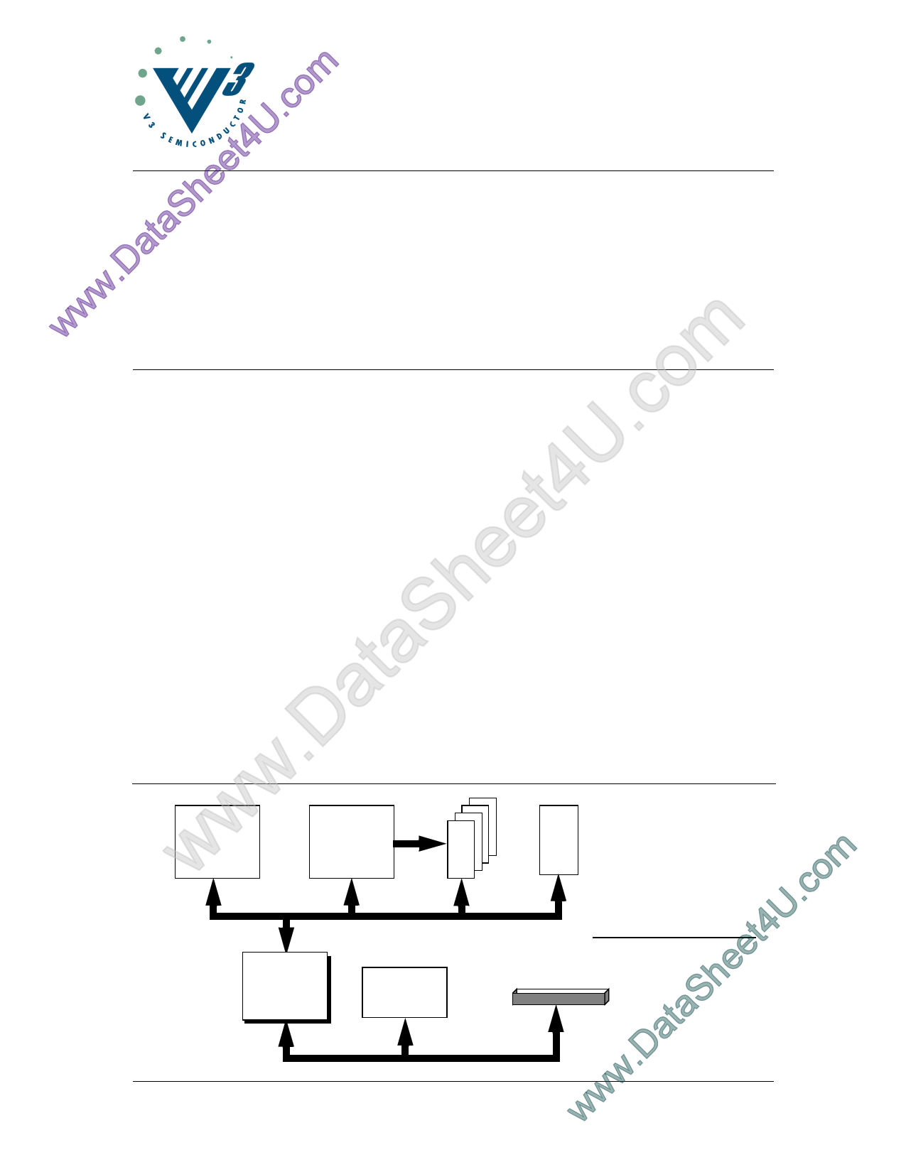
wwi960Cx/Hx/Jx
mCPU
V96BMC
MEMORY
CONTROL
D
R
A
M
ROM
w eet4U.coVxxxEPC
hLOCAL TO
SPCI BRIDGE
PCI
PERIPHERAL
TYPICAL APPLICATION
PCI SLOT or EDGE CONNECTOR
ww.DataCopyright © 1998, V3 Semiconductor Corp.
V96BMC Rev D Data Sheet Rev 3.2
wV3 Semiconductor reserves the right to change the specifications of this product without notice.
1
V96BMC and V96xPBC are trademarks of V3 Semiconductor. All other trademarks are the property of their respective owners.
1 page 
V96BMC Rev.D
PIN #
1
2
3
4
5
6
7
8
9
10
11
12
13
14
15
16
17
18
19
20
21
22
23
24
25
26
27
Signal
A14
A15
A16
Vcc
A17
A19
A20
A18
A21
A24
A22
A23
A26
A25
A27
ALE
-
-
A31
A28
A29
A30
D/C
SUP
PCLK
INT
BERR
Table 4: Pin Assignments
PIN #
34
35
36
37
38
39
40
41
42
43
44
45
46
47
48
49
50
51
52
53
54
55
56
57
58
59
60
Signal
ADS
BE2
BE3
BTERM
READY
ID0
ID1
ID2
RFS/AUXT
LEA
LEB
TXA
TXB
Vcc
GND
HMODE
-
-
-
AA0
AA1
AA2
AA3
Vcc3
GND
AA4
AA5
PIN #
67
68
69
70
71
72
73
74
75
76
77
78
79
80
81
82
83
84
85
86
87
88
89
90
91
92
93
Signal
AA10
AA11
Vcc3
GND
CASA0
CASA1
CASA2
CASA3
Vcc3
GND
RASA0
RASA1
RASA2
RASA3
Vcc3
MWEA
-
-
-
GND
AB0
AB1
AB2
AB3
Vcc3
GND
AB4
PIN #
100
101
102
103
104
105
106
107
108
109
110
111
112
113
114
115
116
117
118
119
120
121
122
123
124
125
126
Signal
AB9
AB10
AB11
Vcc3
GND
CASB0
CASB1
CASB2
CASB3
Vcc3
GND
RASB0
RASB1
RASB2
RASB3
Vcc
-
GND1
MWEB
GND
RESET
A2
A3
A4
A5
A6
A7
Copyright © 1998, V3 Semiconductor Corp.
V96BMC Rev D Data Sheet Rev 3.2
5
5 Page 
V96BMC Rev.D
Table 11: Timing Parameters for V96BMC Vcc=5 Volts +/- 5% and Vcc3= 5 or
3.3 8Volts +/- 5%
Symbol
Description
tC
tCH
tCL
tSU
tH
tH
tRZH
tRHL
tRLH
tRHZ
tBHL
tBLH
tEHL
tELH
tIHL
tILH
tARA1
PCLK period
PCLK high time
PCLK low time
Synchronous input setup
Synchronous input hold
Synchronous input hold (RESET#)
READY 3-state to valid delay
READY synchronous assertion delay
READY synchronous de-assertion delay
READY valid to 3-state delay
BTERM synchronous assertion delay
BTERM synchronous de-assertion delay
BERR synchronous assertion delay
BERR synchronous de-assertion delay
INT synchronous assertion delay
INT synchronous de-assertion delay
Address Input to Row Address output delay
(Interleaved)
tARA2 Address Input to Row Address output delay
(Non-interleaved)
tRAH
tCAV
tCAH
tBCAV
Row address hold from RAS assertion
Column address valid from RAS assertion
Column address hold from CAS assertion
Column address valid delay from previous
CAS assertion (Burst)
tRHL
tRLH
tRAS
tRSH
tRP
tCHL
tCLH
tCAS
tCPN
tRCD
tWESU
PCLK to RAS asserted delay
PCLK to RAS de-asserted delay
RAS pulse width
RAS hold from last CAS assertion
RAS precharge time
PCLK to CAS asserted delay
PCLK to CAS de-asserted delay
CAS pulse width
CAS precharge time
RAS to CAS delay time
Write Enable setup to RAS assertion
Note
1
1
33 MHz
Min Max
30
12
12
9
1
3
3 13
3 13
3 13
3 10
3 14
3 13
3 13
3 12
3 13
3 12
3 14
40 MHz
Min Max Units
25 ns
11 ns
11 ns
8 ns
0.5 ns
3 ns
3 10 ns
3 11 ns
3 11 ns
3 7 ns
3 12 ns
3 11 ns
3 11 ns
3 10 ns
3 11 ns
3 10 ns
3 12 ns
4 18 4 15 ns
2 tM tM+2 tM tM+2 ns
2 tM+1 tM+4 tM+1 tM+4 ns
tC tC ns
tC+3
tC+3 ns
3 13 3 11 ns
3 13 3 11 ns
3 3tC-1
3tC-1
4 tN
tN
5 tP-2
tP-2
1 3 13 3 12
ns
ns
ns
ns
4 12 3 11 ns
4 tN-1
tN-1
ns
0.5tC
0.5tC
ns
1.5tC-2 1.5tC 1.5tC-2 1.5tC ns
10 9 ns
Copyright © 1998, V3 Semiconductor Corp.
V96BMC Rev D Data Sheet Rev 3.2
11
11 Page | ||
| Páginas | Total 14 Páginas | |
| PDF Descargar | [ Datasheet V96BMC.PDF ] | |
Hoja de datos destacado
| Número de pieza | Descripción | Fabricantes |
| V96BMC | High Performance Burst DRAM Controller | V3 Semiconductor |
| Número de pieza | Descripción | Fabricantes |
| SLA6805M | High Voltage 3 phase Motor Driver IC. |
Sanken |
| SDC1742 | 12- and 14-Bit Hybrid Synchro / Resolver-to-Digital Converters. |
Analog Devices |
|
DataSheet.es es una pagina web que funciona como un repositorio de manuales o hoja de datos de muchos de los productos más populares, |
| DataSheet.es | 2020 | Privacy Policy | Contacto | Buscar |