|
|
|
PDF ADF7021 Data sheet ( Hoja de datos )
| Número de pieza | ADF7021 | |
| Descripción | High Performance Narrow-Band Transceiver IC | |
| Fabricantes | Analog Devices | |
| Logotipo | ||
Hay una vista previa y un enlace de descarga de ADF7021 (archivo pdf) en la parte inferior de esta página. Total 30 Páginas | ||
|
No Preview Available !
Data Sheet
High Performance
Narrow-Band Transceiver IC
ADF7021
FEATURES
Low power, narrow-band transceiver
Frequency bands using dual VCO
80 MHz to 650 MHz
862 MHz to 950 MHz
Modulation schemes
2FSK, 3FSK, 4FSK, MSK
Spectral shaping
Gaussian and raised cosine filtering
Data rates supported
0.05 kbps to 32.8 kbps
2.3 V to 3.6 V power supply
Programmable output power
−16 dBm to +13 dBm in 63 steps
Automatic PA ramp control
Receiver sensitivity
−130 dBm at 100 bps, 2FSK
−122 dBm at 1 kbps, 2FSK
−113 dBm at 25 kbps, raised cosine 2FSK
Patent pending, on-chip image rejection calibration
On-chip VCO and fractional-N PLL
On-chip, 7-bit ADC and temperature sensor
Fully automatic frequency control loop (AFC)
Digital received signal strength indication (RSSI)
Integrated Tx/Rx switch
0.1 μA leakage current in power-down mode
APPLICATIONS
Narrow-band standards
ETSI EN 300 220, FCC Part 15, FCC Part 90, FCC Part 95,
ARIB STD-T67
Low cost, wireless data transfer
Remote control/security systems
Wireless metering
Private mobile radio
Wireless medical telemetry service (WMTS)
Keyless entry
Home automation
Process and building control
Pagers
RLNA
RSET
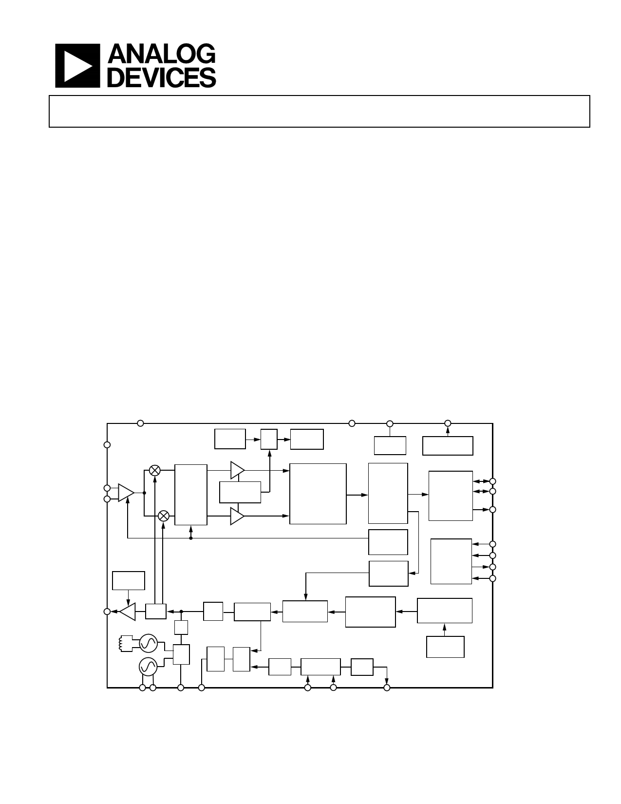
FUNCTIONAL BLOCK DIAGRAM
CE CREG(1:4)
TEMP
SENSOR
MUX
7-BIT ADC
LDO(1:4)
MUXOUT
TEST MUX
RFIN
RFINB
LNA
IF FILTER
RSSI/
LOG AMP
2FSK
3FSK
4FSK
DEMODULATOR
CLOCK
AND DATA
RECOVERY
Tx/Rx
CONTROL
GAIN
PA RAMP
AGC
CONTROL
AFC
CONTROL
SERIAL
PORT
RFOUT
÷1/÷2
VCO1
÷2
DIV P
N/N + 1
Σ-∆
MODULATOR
VCO2
MUX
CP PFD
DIV R
OSC
2FSK
3FSK
4FSK
MOD CONTROL
CLK
DIV
GAUSSIAN/
RAISED COSINE
FILTER
3FSK
ENCODING
TxRxCLK
TxRxDATA
SWD
SLE
SDATA
SREAD
SCLK
L1 L2 VCOIN CPOUT
OSC1 OSC2
Figure 1.
CLKOUT
Rev. D
Document Feedback
Information furnished by Analog Devices is believed to be accurate and reliable. However, no
responsibility is assumed by Analog Devices for its use, nor for any infringements of patents or other
rights of third parties that may result from its use. Specifications subject to change without notice. No
license is granted by implication or otherwise under any patent or patent rights of Analog Devices.
Trademarksandregisteredtrademarksarethepropertyoftheirrespectiveowners.
One Technology Way, P.O. Box 9106, Norwood, MA 02062-9106, U.S.A.
Tel: 781.329.4700 ©2007–2016 Analog Devices, Inc. All rights reserved.
Technical Support
www.analog.com
1 page 
Data Sheet
ADF7021
SPECIFICATIONS
VDD = 2.3 V to 3.6 V, GND = 0 V, TA = TMIN to TMAX, unless otherwise noted. Typical specifications are at VDD = 3 V, TA = 25°C. All
measurements are performed with the EVAL-ADF7021DB evaluation boards using the PN9 data sequence, unless otherwise noted.
RF AND PLL SPECIFICATIONS
Table 1.
Parameter
RF CHARACTERISTICS
Frequency Ranges (Direct Output)
Frequency Ranges (RF Divide-by-2 Mode)
Phase Frequency Detector (PFD) Frequency1
PHASE-LOCKED LOOP (PLL)
VCO Gain2
868 MHz, Internal Inductor VCO
434 MHz, Internal Inductor VCO
426 MHz, External Inductor VCO
160 MHz, External Inductor VCO
Phase Noise (In-Band)
868 MHz, Internal Inductor VCO
433 MHz, Internal Inductor VCO
426 MHz, External Inductor VCO
Phase Noise (Out-of-Band)
Normalized In-Band Phase Noise Floor3
PLL Settling
REFERENCE INPUT
Crystal Reference4
External Oscillator4, 5
Crystal Start-Up Time6
XTAL Bias = 20 µA
XTAL Bias = 35 µA
Input Level for External Oscillator7
OSC1
OSC2
ADC PARAMETERS
INL
DNL
Min
160
862
80
431
RF/256
3.625
3.625
Typ
58
29
27
6
−97
−103
−95
−124
−203
40
0.930
0.438
0.8
CMOS levels
±0.4
±0.4
Max
650
950
325
475
26/30
26
30
Unit
MHz
MHz
MHz
MHz
MHz
MHz/V
MHz/V
MHz/V
MHz/V
dBc/Hz
dBc/Hz
dBc/Hz
dBc/Hz
dBc/Hz
µs
MHz
MHz
ms
ms
V p-p
V
LSB
LSB
Test Conditions/Comments
See Table 9 for required VCO_BIAS and
VCO_ADJUST settings
External inductor VCO
Internal inductor VCO
External inductor VCO, RF divide-by-2 enabled
Internal inductor VCO, RF divide-by-2 enabled
Crystal reference/external reference
VCO_ADJUST = 0, VCO_BIAS = 8
VCO_ADJUST = 0, VCO_BIAS = 8
VCO_ADJUST = 0, VCO_BIAS = 3
VCO_ADJUST = 0, VCO_BIAS = 2
10 kHz offset, PA = 10 dBm, VDD = 3.0 V,
PFD = 19.68 MHz, VCO_BIAS = 8
10 kHz offset, PA = 10 dBm, VDD = 3.0 V,
PFD = 19.68 MHz, VCO_BIAS = 8
10 kHz offset, PA = 10 dBm, VDD = 3.0 V,
PFD = 9.84 MHz, VCO_BIAS = 3
1 MHz offset, fRF = 433 MHz, PA = 10 dBm,
VDD = 3.0 V, PFD = 19.68 MHz, VCO_BIAS = 8
Measured for a 10 MHz frequency step to within
5 ppm accuracy, PFD = 19.68 MHz, loop
bandwidth (LBW) = 100 kHz
10 MHz XTAL, 33 pF load capacitors, VDD = 3.0 V
10 MHz XTAL, 33 pF load capacitors, VDD = 3.0 V
Clipped sine wave
VDD = 2.3 V to 3.6 V, TA = 25°C
VDD = 2.3 V to 3.6 V, TA = 25°C
1 The maximum usable PFD at a particular RF frequency is limited by the minimum N divide value.
2 VCO gain measured at a VCO tuning voltage of 1 V. The VCO gain varies across the tuning range of the VCO. The software package ADIsimPLL™ can be used to model this
variation.
3 This value can be used to calculate the in-band phase noise for any operating frequency. Use the following equation to calculate the in-band phase noise performance
as seen at the PA output: −203 + 10 log(fPFD) + 20 logN.
4 Guaranteed by design. Sample tested to ensure compliance.
5 A TCXO, VCXO, or OCXO can be used as an external oscillator.
6 Crystal start-up time is the time from chip enable (CE) being asserted to correct clock frequency on the CLKOUT pin.
7 Refer to the Reference Input section for details on using an external oscillator.
Rev. D | Page 5 of 62
5 Page 
Data Sheet
ADF7021
GENERAL SPECIFICATIONS
Table 5.
Parameter
TEMPERATURE RANGE (TA)
POWER SUPPLIES
Voltage Supply, VDD
TRANSMIT CURRENT CONSUMPTION1
868 MHz
0 dBm
5 dBm
10 dBm
450 MHz, Internal Inductor VCO
0 dBm
5 dBm
10 dBm
426 MHz, External Inductor VCO
0 dBm
5 dBm
10 dBm
RECEIVE CURRENT CONSUMPTION
868 MHz
Low Current Mode
High Sensitivity Mode
433MHz, Internal Inductor VCO
Low Current Mode
High Sensitivity Mode
426 MHz, External Inductor VCO
Low Current Mode
High Sensitivity Mode
POWER-DOWN CURRENT CONSUMPTION
Low Power Sleep Mode
Min Typ Max Unit Test Conditions/Comments
−40 +85 °C
2.3
3.6 V
All VDD pins must be tied together
VDD = 3.0 V, PA is matched into 50 Ω
VCO_BIAS = 8
20.2 mA
24.7 mA
32.3 mA
VCO_BIAS = 8
19.9 mA
23.2 mA
29.2 mA
VCO_BIAS = 2
13.5 mA
17 mA
23.3 mA
VDD = 3.0 V
VCO_BIAS = 8
22.7 mA
24.6 mA
VCO_BIAS = 8
24.5 mA
26.4 mA
VCO_BIAS = 2
17.5 mA
19.5 mA
0.1 1
µA CE low
1 The transmit current consumption tests used the same combined PA and LNA matching network as that used on the EVAL-ADF7021DB evaluation boards. Improved
PA efficiency is achieved by using a separate PA matching network.
TIMING CHARACTERISTICS
VDD = 3 V ± 10%, DGND = AGND = 0 V, TA = 25°C, unless otherwise noted. Guaranteed by design but not production tested.
Table 6.
Parameter
t1
t2
t3
t4
t5
t6
t8
t9
t10
t11
t12
t13
t14
t15
Limit at TMIN to TMAX
>10
>10
>25
>25
>10
>20
<25
<25
>10
5 < t11 < (¼ × tBIT)
>5
>5
>¼ × tBIT
>¼ × tBIT
Unit Test Conditions/Comments
ns SDATA to SCLK setup time
ns SDATA to SCLK hold time
ns SCLK high duration
ns SCLK low duration
ns SCLK to SLE setup time
ns SLE pulse width
ns SCLK to SREAD data valid, readback
ns SREAD hold time after SCLK, readback
ns SCLK to SLE disable time, readback
ns TxRxCLK negative edge to SLE
ns TxRxDATA to TxRxCLK setup time (Tx mode)
ns TxRxCLK to TxRxDATA hold time (Tx mode)
µs TxRxCLK negative edge to SLE
µs SLE positive edge to positive edge of TxRxCLK
Rev. D | Page 11 of 62
11 Page | ||
| Páginas | Total 30 Páginas | |
| PDF Descargar | [ Datasheet ADF7021.PDF ] | |
Hoja de datos destacado
| Número de pieza | Descripción | Fabricantes |
| ADF7020 | High Performance ISM Band FSK/ASK Transceiver IC | Analog Devices |
| ADF7020-1 | High Performance FSK/ASK Transceiver IC | Analog Devices |
| ADF7021 | High Performance Narrow-Band Transceiver IC | Analog Devices |
| ADF7021-N | High Performance Narrow-Band Transceiver IC | Analog Devices |
| Número de pieza | Descripción | Fabricantes |
| SLA6805M | High Voltage 3 phase Motor Driver IC. |
Sanken |
| SDC1742 | 12- and 14-Bit Hybrid Synchro / Resolver-to-Digital Converters. |
Analog Devices |
|
DataSheet.es es una pagina web que funciona como un repositorio de manuales o hoja de datos de muchos de los productos más populares, |
| DataSheet.es | 2020 | Privacy Policy | Contacto | Buscar |