|
|
PDF ATA5824 Data sheet ( Hoja de datos )
| Número de pieza | ATA5824 | |
| Descripción | (ATA5823 / ATA5824) UHF ASK/FSK Transceiver | |
| Fabricantes | ATMEL Corporation | |
| Logotipo |  |
|
Hay una vista previa y un enlace de descarga de ATA5824 (archivo pdf) en la parte inferior de esta página. Total 30 Páginas | ||
|
No Preview Available !
www.DataSheet4U.com
Features
• Full-duplex Operation Mode without Duplex Frequency Offset to Prevent the Relay
Attack against Passive Entry Go (PEG) Systems
• High FSK Sensitivity: –105.5 dBm at 20 kBaud/–109 dBm at 2.4 kBaud (433.92 MHz)
• High ASK Sensitivity: –111.5 dBm at 10 kBaud/–116 dBm at 2.4 kBaud (100% ASK,
Carrier Level 433.92 MHz)
• Low Supply Current: 10.5 mA in RX and TX Mode (3V/TX with 5 dBm/433.92 MHz)
• Data Rate 1 to 20 kBaud Manchester FSK, 1 to 10 kBaud Manchester
ASK
• ASK/FSK Receiver Uses a Low IF Architecture with High Selectivity,
Blocking and Low Intermodulation (Typical 3 dB Blocking
55.5 dBC at ±750 kHz/60.5 dBC at ±1.5 MHz and 67 dBC at ±10 MHz,
System I1dBCP = –30 dBm/System IIP3 = –20 dBm)
• Wide Bandwidth AGC to Handle Large Outband Blockers above the System I1dBCP
• 226 kHz IF (Intermediate Frequency) with 30 dB Image Rejection and 220 kHz System
Bandwidth to Support TPM Transmitters using ATA5756/ATA5757 Transmitters with
Standard Crystals
• Transmitter Uses Closed Loop FSK Modulation with Fractional-N Synthesizer with
High PLL Bandwidth and an Excellent Isolation between PLL and PA
• Tolerances of XTAL Compensated by Fractional-N Synthesizer with 800 Hz RF
Resolution
• Integrated RX/TX-Switch, Single-ended RF Input and Output
• RSSI (Received Signal Strength Indicator)
• Communication to Microcontroller with SPI Interface Working at 500 kBit/s Maximum
• Configurable Self Polling and RX/TX Protocol Handling with FIFO-RAM Buffering of
Received and Transmitted Data
• 1 Push Button Input and 1 Wake-up Input are Active in Power-down Mode
• Integrated XTAL Capacitors
• PA Efficiency: up to 38% (433.92 MHz/10 dBm/3V)
• Low In-band Sensitivity Change of Typically ±2.0 dB within ±75 kHz Center Frequency
Change in the Complete Temperature and Supply Voltage Range
• Fully Integrated PLL with Low Phase Noise VCO, PLL Loop Filter and full support of
multi-channel operation with arbitrary Channel distance due to Fractional-N
Synthesizer
• Sophisticated Threshold Control and Quasi-peak Detector Circuit in the Data Slicer
• 433.92 MHz, 868.3 MHz and 315 MHz without External VCO and PLL Components
• Efficient XTO Start-up Circuit (> –1.5 kΩ Worst Case Start Impedance)
• Changing of Modulation Type ASK/FSK and Data Rate without Component Changes to
Allow Different Modulation Schemes in TPM and RKE
• Minimal External Circuitry Requirements for Complete System Solution
• Adjustable Output Power: 0 to 10 dBm Adjusted and Stabilized with External Resistor,
Programmable Output Power with 0.5dB Steps with Internal Resistor
• Clock and Interrupt Generation for Microcontroller
• ESD Protection at all Pins (±2.5 kV HBM, ±200V MM, ±500V FCDM)
• Supply Voltage Range: 2.15V to 3.6V or 4.4V to 5.25V
• Typical Power-down Current < 10 nA
• Temperature Range: –40°C to +105°C
• Small 7 mm × 7 mm QFN48 Package
UHF ASK/FSK
Transceiver
ATA5823
ATA5824
Rev. 4829C–RKE–09/05
1 page 
ATA5823/ATA5824
Table 2-1.
Pin
42
43
44
45
46
47
48
Pin Description (Continued)
Symbol
Function
NC Not connected
SCK_POL
Polarity of the serial clock
SCK_PHA
Phase of the serial clock
N_PWR_ON Keyboard input (can also be used to switch on the system, active low)
RX_ACTIVE Indicates RX operation mode
NC Not connected
NC Not connected
GND
Ground/Backplane (exposed die pad)
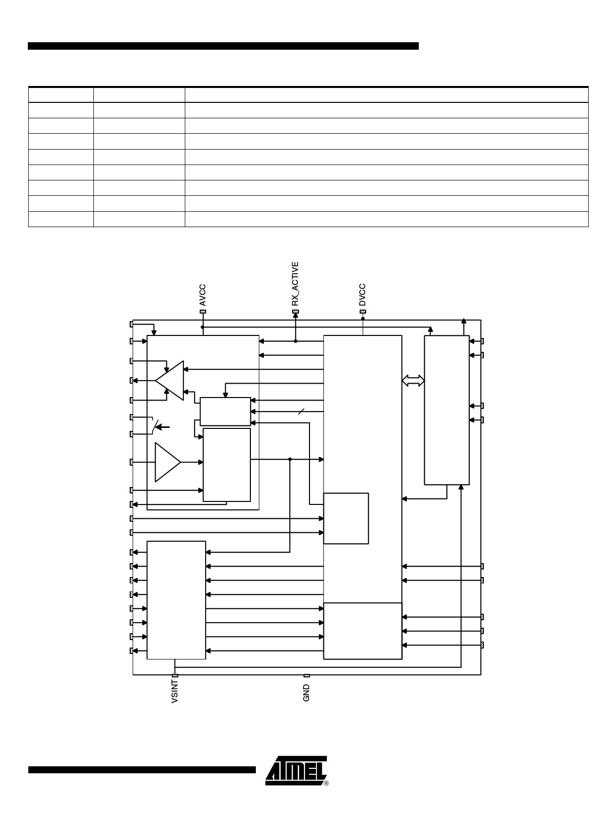
Figure 2-2. Block Diagram
433_N868
SETPWR
R_PWR
RF_OUT
PWR_H
RX_TX1
RX_TX2
RF_IN
CDEM
RSSI
XTAL1
XTAL2
TEST3
CLK
POUT
IRQ
CS
SCK
SDI_TMDI
SDO_TMDO
RF transceiver
PA
RX/TX
switch
LNA
Fract.-N-
Frequency
Synthesizer
Signal
processing
(Mixer
IF-filter
IF-amplifier
FSK/ASK
demodulator
Data filter
Data slicer)
Frontend Enable Digital control logic
PA_Enable (ASK)
TX_DATA (FSK)
RX/TX
FREQ
FREF
13
Demod_Out
TX/RX -
Data buffer
Control register
Status register
Polling circuit
Bit-check logic
Synchronous logic
(Full duplex
operation mode)
XTO
µC_Interface
SPI
Power
Supply
VS2
VS1
Switches
Regulators
Wake-up
Reset
PWR_ON
N_PWR_ON
Reset
TEST1
TEST2
CS_POL
SCK_POL
SCK_PHA
4829C–RKE–09/05
5
5 Page 
ATA5823/ATA5824
A low-IF architecture is also less sensitive to second-order intermodulation (IIP2) than direct
conversion receivers where every pulse or amplitude modulated signal (especially the signals
from TDMA systems like GSM) demodulates to the receiving signal band at second-order
non-linearities.
7.2 Input Matching at RF_IN
The measured input impedances as well as the values of a parallel equivalent circuit of these
impedances can be seen in Table 7-1. The highest sensitivity is achieved with power matching
of these impedances to the source impedance of 50Ω.
Table 7-1. Measured Input Impedances of the RF_IN Pin
fRF/MHz
315
ZIn(RF_IN)
(44-j233)Ω
433.92
(32-j169)Ω
868.3
(21-j78)Ω
RIn_p//CIn_p
1278Ω//2.1 pF
925Ω//2.1 pF
311Ω//2.2 pF
The matching of the LNA Input to 50Ω was done with the circuit according to Figure 7-1 and with
the values of the matching elements given in Table 7-2. The reflection coefficients were always
≤ –10 dB. Note that value changes of C1 and L1 may be necessary to compensate individual
board layout parasitics. The measured typical FSK and ASK Manchester code sensitivities with
a Bit Error Rate (BER) of 10-3 are shown in Table 7-3 on page 12 and Table 7-4 on page 12.
These measurements were done with multilayer inductors having quality factors according to
Table 7-2, resulting in estimated matching losses of 0.8 dB at 315 MHz, 0.8 dB at 433.92 MHz
and 0.7 dB at 868.3 MHz. These losses can be estimated when calculating the parallel equiva-
lent resistance of the inductor with Rloss = 2 × π × f × L × QL and the matching loss with
10 log(1+RIn_p/Rloss).
With an ideal inductor, for example, the sensitivity at 433.92 MHz/FSK/20 kBaud/
±19.5 kHz/Manchester can be improved from –105.5 dBm to –106.7 dBm. The sensitivity also
depends on the values in the registers of the control logic which examines the incoming data
stream. The examination limits must be programmed in control registers 5 and 6. The measure-
ments in Table 7-3 and Table 7-4 on page 12 are based on the values of registers 5 and 6
according to Table 14-3 on page 60.
Figure 7-1. Input Matching to 50Ω
C1 ATA5823/ATA5824
4 RF_IN
L1
4829C–RKE–09/05
11
11 Page | ||
| Páginas | Total 30 Páginas | |
| PDF Descargar | [ Datasheet ATA5824.PDF ] | |
Hoja de datos destacado
| Número de pieza | Descripción | Fabricantes |
| ATA5823 | (ATA5823 / ATA5824) UHF ASK/FSK Transceiver | ATMEL Corporation |
| ATA5824 | (ATA5823 / ATA5824) UHF ASK/FSK Transceiver | ATMEL Corporation |
| Número de pieza | Descripción | Fabricantes |
| SLA6805M | High Voltage 3 phase Motor Driver IC. |
Sanken |
| SDC1742 | 12- and 14-Bit Hybrid Synchro / Resolver-to-Digital Converters. |
Analog Devices |
|
DataSheet.es es una pagina web que funciona como un repositorio de manuales o hoja de datos de muchos de los productos más populares, |
| DataSheet.es | 2020 | Privacy Policy | Contacto | Buscar |
