|
|
|
PDF AD8137 Data sheet ( Hoja de datos )
| Número de pieza | AD8137 | |
| Descripción | Low Power 12-Bit Differential ADC Driver | |
| Fabricantes | Analog Devices | |
| Logotipo | ||
Hay una vista previa y un enlace de descarga de AD8137 (archivo pdf) en la parte inferior de esta página. Total 30 Páginas | ||
|
No Preview Available !
Data Sheet
FEATURES
Fully differential
Extremely low power with power-down feature
2.6 mA quiescent supply current @ 5 V
450 µA in power-down mode @ 5 V
High speed
110 MHz large signal 3 dB bandwidth @ G = 1
450 V/µs slew rate
12-bit SFDR performance @ 500 kHz
Fast settling time: 100 ns to 0.02%
Low input offset voltage: ±2.6 mV max
Low input offset current: 0.45 µA max
Differential input and output
Differential-to-differential or single-ended-to-differential
operation
Rail-to-rail output
Adjustable output common-mode voltage
Externally adjustable gain
Wide supply voltage range: 2.7 V to 12 V
Available in small SOIC package
Qualified for automotive applications
APPLICATIONS
ADC drivers
Automotive vision and safety systems
Automotive infotainment systems
Portable instrumentation
Battery-powered applications
Single-ended-to-differential converters
Differential active filters
Video amplifiers
Level shifters
GENERAL DESCRIPTON
The AD8137 is a low cost differential driver with a rail-to-rail
output that is ideal for driving ADCs in systems that are sensitive
to power and cost. The AD8137 is easy to apply, and its internal
common-mode feedback architecture allows its output common-
mode voltage to be controlled by the voltage applied to one pin.
The internal feedback loop also provides inherently balanced
outputs as well as suppression of even-order harmonic distortion
products. Fully differential and single-ended-to-differential gain
configurations are easily realized by the AD8137. External
feedback networks consisting of four resistors determine the
Low Cost, Low Power,
Differential ADC Driver
AD8137
FUNCTIONAL BLOCK DIAGRAM
–IN 1
VOCM 2
VS+ 3
+OUT 4
AD8137
8 +IN
7 PD
6 VS–
5 –OUT
Figure 1.
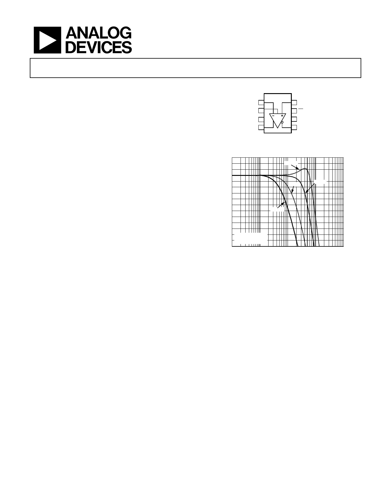
3
2 G=1
1
0
–1 G = 2
G=5
–2
–3
–4
–5
–6 G = 10
–7
–8
–9
–10 RG = 1kΩ
–11 VO, dm = 0.1V p-p
–12
0.1 1
10
FREQUENCY (MHz)
100
Figure 2. Small Signal Response for Various Gains
1000
closed-loop gain of the amplifier. The power-down feature is
beneficial in critical low power applications.
The AD8137 is manufactured on Analog Devices, Inc.,
proprietary second-generation XFCB process, enabling it to
achieve high levels of performance with very low power
consumption.
The AD8137 is available in the small 8-lead SOIC package and
3 mm × 3 mm LFCSP package. It is rated to operate over the
extended industrial temperature range of −40°C to +125°C.
Rev. E
Information furnished by Analog Devices is believed to be accurate and reliable. However, no
responsibility is assumed by Analog Devices for its use, nor for any infringements of patents or other
rights of third parties that may result from its use. Specifications subject to change without notice. No
license is granted by implication or otherwise under any patent or patent rights of Analog Devices.
Trademarksandregisteredtrademarksarethepropertyoftheirrespectiveowners.
One Technology Way, P.O. Box 9106, Norwood, MA 02062-9106, U.S.A.
Tel: 781.329.4700
www.analog.com
Fax: 781.461.3113 ©2004–2012 Analog Devices, Inc. All rights reserved.
1 page 
AD8137
Parameter
Input Bias Current
CMRR
Power Supply
Operating Range
Quiescent Current
Quiescent Current, Disabled
PSRR
PD Pin
Threshold Voltage
Input Current
OPERATING TEMPERATURE RANGE
Conditions
AD8137W only: TMIN-TMAX
ΔVO, dm/ΔVOCM, ΔVOCM = ±0.5 V
AD8137W only: TMIN-TMAX
AD8137W only: TMIN-TMAX
AD8137W only: TMIN-TMAX
Power-down = low
AD8137W only: TMIN-TMAX
ΔVS = ±1 V
AD8137W only: TMIN-TMAX
AD8137W only: TMIN-TMAX
Power-down = high/low
AD8137W only: TMIN-TMAX
Data Sheet
Min
62
62
+2.7
+2.7
79
79
VS− + 0.7
VS− + 0.7
−40
Typ Max
0.3 1.1
1.1
75
±6
±6
3.2 3.60
3.65
750 900
900
91
150/210
VS− + 1.7
VS− + 1.7
170/240
180/245
+125
Unit
µA
µA
dB
dB
V
V
mA
mA
µA
µA
dB
dB
V
V
µA
µA
°C
Rev. E | Page 4 of 32
5 Page 
AD8137
PIN CONFIGURATION AND FUNCTION DESCRIPTIONS
Data Sheet
–IN 1
VOCM 2
VS+ 3
+OUT 4
AD8137
8 +IN
7 PD
6 VS–
5 –OUT
Figure 4. Pin Configuration
Table 6. Pin Function Descriptions
Pin No.
Mnemonic
Description
1 −IN
Inverting Input.
2 VOCM
An internal feedback loop drives the output common-mode voltage to be equal to the voltage applied to
the VOCM pin, provided the operation of the amplifier remains linear.
3 VS+
Positive Power Supply Voltage.
4 +OUT Positive Side of the Differential Output.
5 −OUT Negative Side of the Differential Output.
6 VS−
7 PD
Negative Power Supply Voltage.
Power Down.
8 +IN
Noninverting Input.
EPAD
Exposed paddle may be connected to either ground plane or power plane.
Rev. E | Page 10 of 32
11 Page | ||
| Páginas | Total 30 Páginas | |
| PDF Descargar | [ Datasheet AD8137.PDF ] | |
Hoja de datos destacado
| Número de pieza | Descripción | Fabricantes |
| AD813 | Low Power Triple Video Amplifier | Analog Devices |
| AD8130 | (AD8129 / AD8130) Low Cost 270 MHz Differential Receiver Amplifiers | Analog Devices |
| AD8131 | Low-Cost / High-Speed Differential Driver | Analog Devices |
| AD8132 | Low-Cost/ High-Speed Differential Amplifier | Analog Devices |
| Número de pieza | Descripción | Fabricantes |
| SLA6805M | High Voltage 3 phase Motor Driver IC. |
Sanken |
| SDC1742 | 12- and 14-Bit Hybrid Synchro / Resolver-to-Digital Converters. |
Analog Devices |
|
DataSheet.es es una pagina web que funciona como un repositorio de manuales o hoja de datos de muchos de los productos más populares, |
| DataSheet.es | 2020 | Privacy Policy | Contacto | Buscar |