|
|
|
PDF ZL50010 Data sheet ( Hoja de datos )
| Número de pieza | ZL50010 | |
| Descripción | Flexible 512 Channel DX | |
| Fabricantes | Zarlink Semiconductor | |
| Logotipo | ||
Hay una vista previa y un enlace de descarga de ZL50010 (archivo pdf) en la parte inferior de esta página. Total 30 Páginas | ||
|
No Preview Available !
www.DataSheet4U.com
ZL50010
Flexible 512 Channel DX with Enhanced
DPLL
Data Sheet
Features
• 512 channel x 512 channel non-blocking switch
at 2.048 Mbps, 4.096 Mbps or 8.192 Mbps
operation
• Rate conversion between the ST-BUS inputs and
ST-BUS outputs
• Integrated Digital Phase-Locked Loop (DPLL)
meets Telcordia GR-1244-CORE Stratum 4
enhanced specifications
• DPLL provides automatic reference switching,
jitter attenuation, holdover and free run functions
• Per-stream ST-BUS input with data rate selection
of 2.048 Mbps, 4.096 Mbps or 8.192 Mbps
• Per-stream ST-BUS output with data rate
selection of 2.048 Mbps, 4.096 Mbps or
8.192 Mbps; the output data rate can be different
than the input data rate
• Per-stream high impedance control output for
every ST-BUS output with fractional bit
advancement
• Per-stream input channel and input bit delay
programming with fractional bit delay
July 2004
Ordering Information
ZL50010/QCC 160 Pin LQFP
ZL50010/GDC 144 Ball LBGA
-40°C to +85°C
• Per-stream output channel and output bit delay
programming with fractional bit advancement
• Multiple frame pulse outputs and reference clock
outputs
• Per-channel constant throughput delay
• Per-channel high impedance output control
• Per-channel message mode
• Per-channel Pseudo Random Bit Sequence
(PRBS) pattern generation and bit error detection
• Control interface compatible to Motorola non-
multiplexed CPUs
• Connection memory block programming
capability
• IEEE-1149.1 (JTAG) test port
• 3.3 V I/O with 5 V tolerant input
VDD VSS RESET
ODE
STi0-15
FPi
CKi
PRI_REF
SEC_REF
S/P Converter
Input Timing
Data Memory
Connection Memory
DPLL
OSC
APLL
Microprocessor
Interface
and
Internal
Registers
P/S Converter
STo0-15
Output HiZ Control
Output Timing
Test Port
STOHZ0-15
FPo0
CKo0
FPo1
CKo1
FPo2
CKo2
IC0 - 4
CLKBYPS
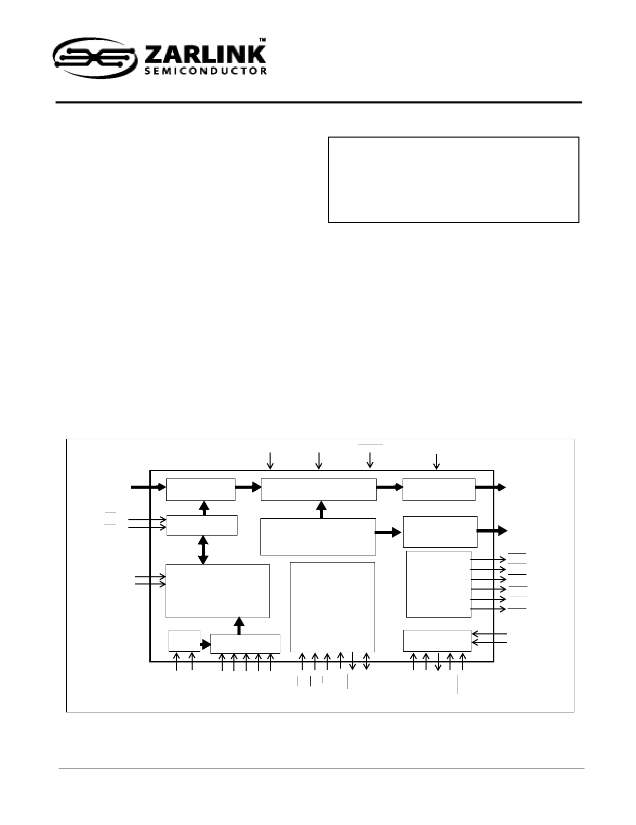
Figure 1 - ZL50010 Functional Block Diagram
Zarlink Semiconductor US Patent No. 5,602,884, UK Patent No. 0772912,
France Brevete S.G.D.G. 0772912; Germany DBP No. 69502724.7-08
1
Zarlink Semiconductor Inc.
Zarlink, ZL and the Zarlink Semiconductor logo are trademarks of Zarlink Semiconductor Inc.
Copyright 2003-2004, Zarlink Semiconductor Inc. All Rights Reserved.
1 page 
ZL50010
Data Sheet
List of Figures
Figure 1 - ZL50010 Functional Block Diagram . . . . . . . . . . . . . . . . . . . . . . . . . . . . . . . . . . . . . . . . . . . . . . . . . . . . 1
Figure 2 - 24 mm x 24 mm LQFP (JEDEC MS-026) Pinout Diagram . . . . . . . . . . . . . . . . . . . . . . . . . . . . . . . . . . . 8
Figure 3 - 13 mm x 13 mm 144 Ball LBGA Pinout Diagram. . . . . . . . . . . . . . . . . . . . . . . . . . . . . . . . . . . . . . . . . . . 9
Figure 4 - Input Timing when (CKIN2 to CKIN0 Bits = 010) in the Control Register . . . . . . . . . . . . . . . . . . . . . . . 16
Figure 5 - Input Timing when (CKIN2 to CKIN0 Bits = 001) in the Control Register . . . . . . . . . . . . . . . . . . . . . . . 16
Figure 6 - Input Timing when (CKIN2 to CKIN0 Bits = 000) in the Control Register . . . . . . . . . . . . . . . . . . . . . . . 16
Figure 7 - ST-BUS Input Timing for Various Input Data Rates . . . . . . . . . . . . . . . . . . . . . . . . . . . . . . . . . . . . . . . . 17
Figure 8 - FPo0 and CKo0 Output Timing when the CKFP0 Bit = 0 . . . . . . . . . . . . . . . . . . . . . . . . . . . . . . . . . . . 19
Figure 9 - FPo0 and CKo0 Output Timing when the CKFP0 Bit = 1 . . . . . . . . . . . . . . . . . . . . . . . . . . . . . . . . . . . 19
Figure 10 - FPo1 and CKo1 Output Timing when the CKFP1 Bit = 0 . . . . . . . . . . . . . . . . . . . . . . . . . . . . . . . . . . 19
Figure 11 - FPo1 and CKo1 Output Timing when the CKFP1 Bit = 1 . . . . . . . . . . . . . . . . . . . . . . . . . . . . . . . . . . 19
Figure 12 - FPo2 and CKo2 Output Timing when the CKFP2 Bit = 0 . . . . . . . . . . . . . . . . . . . . . . . . . . . . . . . . . . 20
Figure 13 - FPo2 and CKo2 Output Timing when the CKFP2 Bit = 1 . . . . . . . . . . . . . . . . . . . . . . . . . . . . . . . . . . 20
Figure 14 - ST-BUS Output Timing for Various Output Data Rates . . . . . . . . . . . . . . . . . . . . . . . . . . . . . . . . . . . . 21
Figure 15 - Input Channel Delay Timing Diagram . . . . . . . . . . . . . . . . . . . . . . . . . . . . . . . . . . . . . . . . . . . . . . . . . 22
Figure 16 - Input Bit Delay Timing Diagram . . . . . . . . . . . . . . . . . . . . . . . . . . . . . . . . . . . . . . . . . . . . . . . . . . . . . . 23
Figure 17 - Output Channel Delay Timing Diagram . . . . . . . . . . . . . . . . . . . . . . . . . . . . . . . . . . . . . . . . . . . . . . . . 23
Figure 18 - Output Bit Delay Timing Diagram . . . . . . . . . . . . . . . . . . . . . . . . . . . . . . . . . . . . . . . . . . . . . . . . . . . . 24
Figure 19 - Fractional Output Bit Advancement Timing Diagram. . . . . . . . . . . . . . . . . . . . . . . . . . . . . . . . . . . . . . 24
Figure 20 - Example: External High Impedance Control Timing . . . . . . . . . . . . . . . . . . . . . . . . . . . . . . . . . . . . . . 25
Figure 21 - Data Throughput Delay when Input and Output Channel Delay are Disabled for Input Ch0 Switched to
Output Ch0 . . . . . . . . . . . . . . . . . . . . . . . . . . . . . . . . . . . . . . . . . . . . . . . . . . . . . . . . . . . . . . . . . . . . . . 27
Figure 22 - Data Throughput Delay when Input Channel Delay is Enabled and Output Channel Delay is Disabled
for Input Ch0 Switched to Output Ch0 . . . . . . . . . . . . . . . . . . . . . . . . . . . . . . . . . . . . . . . . . . . . . . . . . 27
Figure 23 - Data Throughput Delay when Input Channel Delay is Disabled and Output Channel Delay is Enabled
for Input Ch0 Switch to Output Ch0 . . . . . . . . . . . . . . . . . . . . . . . . . . . . . . . . . . . . . . . . . . . . . . . . . . . 27
Figure 24 - Data Throughput Delay when Input and Output Channel Delay are Enabled for Input Ch0 Switched to
Output Ch0 . . . . . . . . . . . . . . . . . . . . . . . . . . . . . . . . . . . . . . . . . . . . . . . . . . . . . . . . . . . . . . . . . . . . . . 28
Figure 25 - DPLL Functional Block Diagram . . . . . . . . . . . . . . . . . . . . . . . . . . . . . . . . . . . . . . . . . . . . . . . . . . . . . 35
Figure 26 - Skew Control Circuit Diagram . . . . . . . . . . . . . . . . . . . . . . . . . . . . . . . . . . . . . . . . . . . . . . . . . . . . . . . 36
Figure 27 - State Machine Diagram . . . . . . . . . . . . . . . . . . . . . . . . . . . . . . . . . . . . . . . . . . . . . . . . . . . . . . . . . . . . 37
Figure 28 - Block Diagram of the PLL Module . . . . . . . . . . . . . . . . . . . . . . . . . . . . . . . . . . . . . . . . . . . . . . . . . . . . 38
Figure 29 - DPLL Jitter Transfer Function Diagram - Wide Range of Frequencies . . . . . . . . . . . . . . . . . . . . . . . . 41
Figure 30 - Detailed DPLL Jitter Transfer Function Diagram (Wander Transfer Diagram) . . . . . . . . . . . . . . . . . . 41
Figure 31 - Crystal Oscillator Circuit . . . . . . . . . . . . . . . . . . . . . . . . . . . . . . . . . . . . . . . . . . . . . . . . . . . . . . . . . . . 44
Figure 32 - External Clock Oscillator Circuit . . . . . . . . . . . . . . . . . . . . . . . . . . . . . . . . . . . . . . . . . . . . . . . . . . . . . 45
Figure 33 - Frame Pulse Input and Clock Input Timing Diagram . . . . . . . . . . . . . . . . . . . . . . . . . . . . . . . . . . . . . . 72
Figure 34 - Frame Boundary Timing with Input Clock (Cycle-to-Cycle) Variation . . . . . . . . . . . . . . . . . . . . . . . . . 72
Figure 35 - Frame Boundary Timing with Input Frame Pulse (Cycle-to-Cycle) Variation. . . . . . . . . . . . . . . . . . . . 73
Figure 36 - XTALi Input Timing Diagram when Clock Oscillator is Connected . . . . . . . . . . . . . . . . . . . . . . . . . . . 73
Figure 37 - Reference Input Timing Diagram when the Input Frequency = 8 kHz . . . . . . . . . . . . . . . . . . . . . . . . . 74
Figure 38 - Reference Input Timing Diagram when the Input Frequency = 2.048 MHz. . . . . . . . . . . . . . . . . . . . . 74
Figure 39 - Reference Input Timing Diagram when the Input Frequency = 1.544 Hz . . . . . . . . . . . . . . . . . . . . . . 74
Figure 40 - Input and Output Frame Boundary Offset . . . . . . . . . . . . . . . . . . . . . . . . . . . . . . . . . . . . . . . . . . . . . . 75
Figure 41 - FPo0 and CKo0 Timing Diagram. . . . . . . . . . . . . . . . . . . . . . . . . . . . . . . . . . . . . . . . . . . . . . . . . . . . . 76
Figure 42 - FPo1 and CKo1 Timing Diagram. . . . . . . . . . . . . . . . . . . . . . . . . . . . . . . . . . . . . . . . . . . . . . . . . . . . . 77
Figure 43 - FPo2 and CKo2 Timing Diagram. . . . . . . . . . . . . . . . . . . . . . . . . . . . . . . . . . . . . . . . . . . . . . . . . . . . . 78
Figure 44 - ST-BUS Inputs (STi0 - 15) Timing Diagram. . . . . . . . . . . . . . . . . . . . . . . . . . . . . . . . . . . . . . . . . . . . . 79
Figure 45 - ST-BUS Outputs (STo0 - 15) Timing Diagram . . . . . . . . . . . . . . . . . . . . . . . . . . . . . . . . . . . . . . . . . . . 80
5
Zarlink Semiconductor Inc.
5 Page 
ZL50010
Data Sheet
Pin Description (continued)
LQFP Pin
Number
12
LBGA Ball
Number
A9
Name
TM1
13 C10 TM2
14, 15
16
17
C9, C8
D8
B8
NC1, NC2
Vss_APLL
VDD_APLL
19 A8 XTALo
20 A7 XTALi
22
24 - 28
30
B7
A6, A5, B6,
B5, C7
C4
CLKBYPS
IC0 - 4
PRI_REF
31 A4 SEC_REF
Description
APLL Test Pin 1: For normal operation, this input MUST be
low.
APLL Test Pin 2: For normal operation, this input MUST be
low.
No Connection: These pins MUST be left unconnected.
Ground for the APLL Circuit.
Power Supply for the on-chip Analog Phase-Locked Loop
(APLL) Circuit: +3.3 V
Oscillator Clock Output (3.3 V Output). This pin is connected
to a 20 MHz crystal (see Figure 31 on page 44), or it is left
unconnected if a clock oscillator is connected to the XTALi pin
(see Figure 32 on page 45). If the device is to be used in DPLL
Bypass mode only, the crystal or clock oscillator can be
omitted, in which case this pin must be left unconnected.
Oscillator Clock Input (3.3 V Input). This pin is connected to
a 20 MHz crystal (see Figure 31 on page 44), or it is connected
to a clock oscillator (see Figure 32 on page 45). If the device is
to be used in DPLL Bypass mode only, the crystal or clock
oscillator can be omitted, in which case this pin must be held
low.
Test Clock Input: For device testing only, in normal operation,
this input MUST be low.
Internal connection (3.3 V Tolerant Inputs with internal
pull-down):
In normal mode, these pins must be low.
Primary Reference Input (5 V Tolerant Input): This pin
accepts an 8 kHz, 1.544 MHz or 2.048 MHz timing reference. It
is used as one of the primary references for the DPLL in the
Master mode. This pin is ignored in the DPLL Freerun or
Bypass Mode.
When this pin is not in use, it is required to be driven high or
low by connecting it to Vdd or ground through an external pull-
up resistor or external pull-down resistor.
Secondary Reference Input (5 V Tolerant Inputs): This pins
accept an 8 kHz, 1.544 MHz or 2.048 MHz timing reference. It
is used as the secondary reference for the DPLL in the Master
mode. This pin is ignored in the DPLL Freerun or Bypass
Mode.
When this pin is not in use, it is required to be driven high or
low by connecting it to Vdd ground, through an external pull-up
resistor or external pull-down resistor.
11
Zarlink Semiconductor Inc.
11 Page | ||
| Páginas | Total 30 Páginas | |
| PDF Descargar | [ Datasheet ZL50010.PDF ] | |
Hoja de datos destacado
| Número de pieza | Descripción | Fabricantes |
| ZL50010 | Flexible 512 Channel DX | Zarlink Semiconductor |
| ZL50011 | Flexible 512 Channel DX | Zarlink Semiconductor |
| ZL50012 | Flexible 512-ch Digital Switch | Zarlink Semiconductor |
| ZL50015 | Enhanced 1 K Digital Switch | Zarlink Semiconductor |
| Número de pieza | Descripción | Fabricantes |
| SLA6805M | High Voltage 3 phase Motor Driver IC. |
Sanken |
| SDC1742 | 12- and 14-Bit Hybrid Synchro / Resolver-to-Digital Converters. |
Analog Devices |
|
DataSheet.es es una pagina web que funciona como un repositorio de manuales o hoja de datos de muchos de los productos más populares, |
| DataSheet.es | 2020 | Privacy Policy | Contacto | Buscar |