|
|
|
PDF ADM1192 Data sheet ( Hoja de datos )
| Número de pieza | ADM1192 | |
| Descripción | Digital Power Monitor | |
| Fabricantes | Analog Devices | |
| Logotipo | ||
Hay una vista previa y un enlace de descarga de ADM1192 (archivo pdf) en la parte inferior de esta página. Total 21 Páginas | ||
|
No Preview Available !
Data Sheet
Digital Power Monitor
with Clear Pin and ALERT Output
ADM1192
FEATURES
Powered from 3.15 V to 26 V
Precision current sense amplifier
Precision voltage input
12-bit ADC for current and voltage readback
ALERT output allows basic P-channel FET hot swap up to 26 V
SETV input for setting overcurrent alert threshold
Programmable overcurrent filtering via TIMER pin
CLRB input pin
I2C fast mode-compliant interface (400 kHz maximum)
10-lead MSOP
APPLICATIONS
Power monitoring/power budgeting
Central office equipment
Telecommunications and data communications equipment
PCs/servers
GENERAL DESCRIPTION
The ADM1192 is an integrated current sense amplifier that
offers digital current and voltage monitoring via an on-chip
12-bit analog-to-digital converter (ADC), communicated
through an I2C® interface.
An internal current sense amplifier measures voltage across the
sense resistor in the power path via the VCC pin and the SENSE pin.
A 12-bit ADC can measure the current seen in the sense resistor
and in the supply voltage on the VCC pin. An industry-standard
I2C interface allows a controller to read current and voltage
data from the ADC. Measurements can be initiated by an I2C
command. Alternatively, the ADC can run continuously, and
the user can read the latest conversion data whenever it is
required. Up to four unique I2C addresses can be created,
depending on the way the ADR pin is connected.
A SETV pin is also included. A voltage applied to this pin is
internally compared with the output voltage on the current sense
amplifier. The output of the SETV comparator asserts when the
current sense amplifier output exceeds the SETV voltage. This
event is detected at the ALERT block. The ALERT block then
charges up the external TIMER capacitor with a fixed current.
When this timing cycle is complete, the ALERT output asserts.
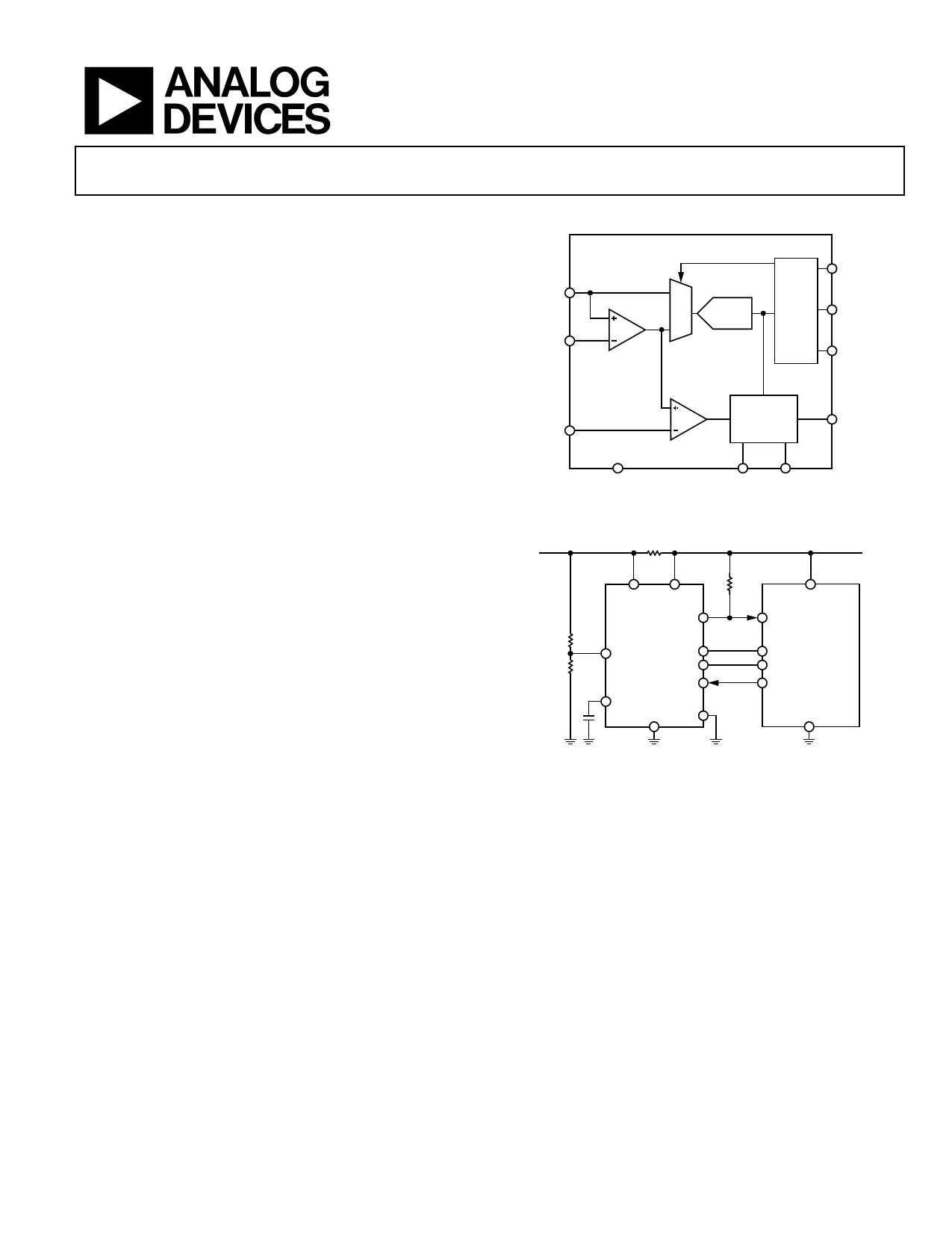
FUNCTIONAL BLOCK DIAGRAM
ADM1192
VCC
SENSE
V
0
I
A1
CURRENT
SENSE
AMPLIFIER
MUX
12-BIT
ADC
SDA
I2C SCL
ADR
SETV
COMPARATOR
ALERT
GND
CLRB TIMER
Figure 1.
ALERT
3.15V TO 26V
RSENSE
VCC SENSE
ALERT
ADM1192
SETV
SDA
SCL
CLRB
TIMER
GND ADR
CONTROLLER
INTERRUPT
P = VI
SDA
SCL
CLRB
Figure 2. Applications Diagram
The ALERT output can be used as a flag to warn a micro-
controller or field programmable gate array (FPGA) of an
overcurrent condition. ALERT outputs of multiple ADM1192
devices can be tied together and used as a combined alert.
A basic P-channel FET hot swap circuit can be implemented
with the ALERT output. The value of the TIMER capacitor
should be set so that the charging time of this capacitor is much
longer than the period during which a higher than nominal
inrush current may be flowing.
The ADM1192 is packaged in a 10-lead MSOP.
Rev. D
Document Feedback
Information furnished by Analog Devices is believed to be accurate and reliable. However, no
responsibility is assumed by Analog Devices for its use, nor for any infringements of patents or other
rights of third parties that may result from its use. Specifications subject to change without notice. No
license is granted by implication or otherwise under any patent or patent rights of Analog Devices.
Trademarksandregisteredtrademarksarethepropertyoftheirrespectiveowners.
One Technology Way, P.O. Box 9106, Norwood, MA 02062-9106, U.S.A.
Tel: 781.329.4700 ©2006–2013 Analog Devices, Inc. All rights reserved.
Technical Support
www.analog.com
1 page 
ADM1192
Data Sheet
Parameter
TIMER PIN
Pull-Up Current (Overcurrent Fault), ITIMERUPOC
Pull-Down Current, ITIMERDN
Pin Threshold High, VTIMERH
ALERT PIN
Output Low Voltage, VALERTOL
Input Current, IALERT
ADR PIN
Set Address to 00, VADRLOWV
Set Address to 01, RADRLOWZ
Set Address to 10, IADRHIGHZ
Set Address to 11, VADRHIGHV
Input Current for 00 Decode, IADRLOW
Input Current for 11 Decode, IADRHIGH
I2C TIMING
Low Level Input Voltage, VIL
High Level Input Voltage, VIH
Low Level Output Voltage on SDA, VOL
Output Fall Time on SDA from VIHMIN to VILMAX
Maximum Width of Spikes Suppressed by
Input Filtering on SDA Pin and SCL Pin
Input Current, II, on SDA/SCL When Not
Driving a Logic Low Output
Input Capacitance on SDA/SCL
SCL Clock Frequency, fSCL
Low Period of the SCL Clock
High Period of the SCL Clock
Setup Time for Repeated Start Condition, tSU;STA
SDA Output Data Hold Time, tHD;DAT
Setup Time for a Stop Condition, tSU;STO
Bus Free Time Between a Stop and a Start
Condition, tBUF
Capacitive Load for Each Bus Line
Min
−46
1.275
−1
0
80
−0.3
2
−40
Typ
−62
100
1.3
0.05
1
120
−25
3
0.7 VBUS
20 + 0.1 CBUS
50
−10
5
600
1300
600
100
600
1300
Max Unit Test Conditions/Comments
−78 µA (18.125 × VSENSE) > VSETV, VTIMER = 1 V
µA Normal operation, VTIMER = 1 V
1.325 V
TIMER rising
0.1 V IALERT = −100 µA
1.5 mA IALERT = −2 mA
+1 µA VALERT = VCC; ALERT asserted
0.8 V Low state
160 kΩ Resistor to ground state, load pin with
specified resistance for 01 decode
+0.3 µA Open state, maximum load allowed on
ADR pin for 10 decode
5.5 V High state
µA VADR = 0 V to 0.8 V
6 µA VADR = 2.0 V to 5.5 V
0.3 VBUS
0.4
250
250
V
V
V
ns
ns
VBUS = 3.0 V to 5.5 V
VBUS = 3.0 V to 5.5 V
IOL = 3 mA
CBUS = bus capacitance from SDA to GND
+10 µA
pF
400 kHz
ns
ns
ns
900 ns
ns
ns
400 pF
1 Monitoring accuracy is a measure of the error in a code that is read back for a particular voltage/current. This is a combination of amplifier error, reference error, ADC
error, and error in ADC full-scale code conversion factor.
2 This is an absolute value to be used when converting ADC codes to current readings; any inaccuracy in this value is factored into absolute current accuracy values (see the
Specifications for the Current Sense Absolute Accuracy parameter).
3 These are absolute values to be used when converting ADC codes to voltage readings; any inaccuracy in these values is factored into voltage accuracy values (see the
Specifications for the Voltage Sense Accuracy parameter).
4 Time between the receipt of the command byte and the actual ADC result being placed in the register.
Rev. D | Page 4 of 20
5 Page 
ADM1192
VOLTAGE AND CURRENT READBACK
The ADM1192 contains the components to allow voltage and
current readback over an I2C bus. The voltage output of the
current sense amplifier and the voltage on the VCC pin are fed
into a 12-bit ADC via a multiplexer. The device can be instructed
to convert voltage and/or current at any time during operation
via an I2C command. When all conversions are complete, the
voltage and/or current values can be read back with 12-bit
accuracy in two or three bytes.
SERIAL BUS INTERFACE
Control of the ADM1192 is carried out via the serial system
management bus (I2C). This interface is compatible with the I2C
fast mode (400 kHz maximum). The ADM1192 is connected to
this bus as a slave device, under the control of a master device.
IDENTIFYING THE ADM1192 ON THE I2C BUS
The ADM1192 has a 7-bit serial bus slave address. When the
device powers up, it does so with a default serial bus address.
The five MSBs of the address are set to 01011; the two LSBs are
determined by the state of the ADR pin. There are four config-
urations available on the ADR pin that correspond to four I2C
addresses for the two LSBs (see Table 5). This scheme allows four
ADM1192 devices to operate on a single I2C bus.
GENERAL I2C TIMING
Figure 18 and Figure 19 show timing diagrams for general write
and read operations using the I2C. The I2C specification defines
conditions for different types of read and write operations, which
are discussed in the Write and Read Operations section. The
general I2C protocol operates as follows:
1. The master initiates a data transfer by establishing a start
condition, defined as a high-to-low transition on the serial
data line, SDA, while the serial clock line, SCL, remains
high. This indicates that a data stream is to follow. All slave
peripherals connected to the serial bus respond to the start
condition and shift in the next eight bits, consisting of a 7-bit
slave address (MSB first) plus an R/W bit that determines the
direction of the data transfer, that is, whether data is written to
or read from the slave device (0 = write, 1 = read).
Data Sheet
The peripheral whose address corresponds to the transmitted
address responds by pulling the data line low during the
low period before the ninth clock pulse, known as the
acknowledge bit, and holding it low during the high period
of this clock pulse. All other devices on the bus now remain
idle while the selected device waits for data to be read from
it or written to it. If the R/W bit is 0, the master writes to
the slave device. If the R/W bit is 1, the master reads from
the slave device.
2. Data is sent over the serial bus in sequences of nine clock
pulses: eight bits of data followed by an acknowledge bit
from the slave device. Data transitions on the data line must
occur during the low period of the clock signal and remain
stable during the high period because a low-to-high transition
when the clock is high can be interpreted as a stop signal.
If the operation is a write operation, the first data byte after
the slave address is a command byte. This tells the slave
device what to expect next. It can be an instruction, such as
telling the slave device to expect a block write, or it can be
a register address that tells the slave where subsequent data
is to be written.
Because data can flow in only one direction, as defined by
the R/W bit, it is not possible to send a command to a slave
device during a read operation. Before performing a read
operation, it may be necessary to first execute a write
operation to tell the slave what sort of read operation to
expect and/or the address from which data is to be read.
3. When all data bytes are read or written, stop conditions are
established. In write mode, the master pulls the data line
high during the 10th clock pulse to assert a stop condition.
In read mode, the master device releases the SDA line
during the SCL low period before the ninth clock pulse,
but the slave device does not pull it low. This is known as a
no acknowledge. The master then takes the data line low
during the SCL low period before the 10th clock pulse, and
then high during the 10th clock pulse to assert a stop
condition.
Table 5. Setting I2C Addresses via the ADR Pin
Base Address
ADR Pin State
01011
Ground
Resistor to ground
Floating
High
1 X = don’t care.
ADR Pin Logic State
00
01
10
11
Address in Binary1
0101100X
0101101X
0101110X
0101111X
Address in Hex
0x58
0x5A
0x5C
0x5E
Rev. D | Page 10 of 20
11 Page | ||
| Páginas | Total 21 Páginas | |
| PDF Descargar | [ Datasheet ADM1192.PDF ] | |
Hoja de datos destacado
| Número de pieza | Descripción | Fabricantes |
| ADM1191 | Digital Power Monitor | Analog Devices |
| ADM1192 | Digital Power Monitor | Analog Devices |
| Número de pieza | Descripción | Fabricantes |
| SLA6805M | High Voltage 3 phase Motor Driver IC. |
Sanken |
| SDC1742 | 12- and 14-Bit Hybrid Synchro / Resolver-to-Digital Converters. |
Analog Devices |
|
DataSheet.es es una pagina web que funciona como un repositorio de manuales o hoja de datos de muchos de los productos más populares, |
| DataSheet.es | 2020 | Privacy Policy | Contacto | Buscar |