|
|
|
PDF NB4N441 Data sheet ( Hoja de datos )
| Número de pieza | NB4N441 | |
| Descripción | 3.3V Serial Input MultiProtocol PLL Clock Synthesizer | |
| Fabricantes | ON Semiconductor | |
| Logotipo | ||
Hay una vista previa y un enlace de descarga de NB4N441 (archivo pdf) en la parte inferior de esta página. Total 12 Páginas | ||
|
No Preview Available !
NB4N441
3.3V Serial Input
MultiProtocol PLL Clock
Synthesizer, Differential
LVPECL Output
Description
The NB4N441 is a precision clock synthesizer which generates a
differential LVPECL clock output frequency from 12.5 MHz to
425 MHz. A Serial Peripheral Interface (SPI) is used to configure the
device to produce one of sixteen popular standard protocol output
frequencies from a single 27 MHz crystal reference. The NB4N441
also has the added feature of allowing application specific output
frequencies from 12.5 MHz to 425 MHz using crystals within the
range of 10 MHz to 28 MHz.
Features
• Performs Precision Clock Generation and Synthesis from a Single
27 MHz Crystal Reference
• Serial Load Capability for Proprietary Frequencies
• Flexible Input Allows for External Clock Reference
• Exceeds Bellcore and ITU Jitter Generation Specification
• PLL Lock Detect Output
• Output Enable
• Fully Integrated Phase−Lock−Loop with Internal Loop Filter
• Operating Range: VCC = 3.135 V to 3.465 V
• Small Footprint 24 Pin QFN
• These are Pb−Free Devices*
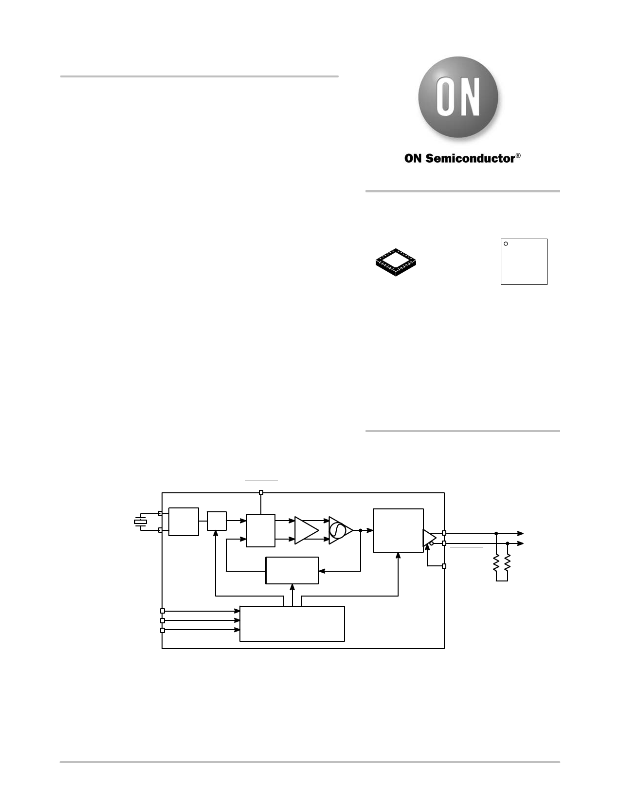
LOCKED
27 MHz
XTAL
OSC
B
R
FB
Feedback
Divider
SDATA
SCLOCK
SLOAD
Frequency Control Logic
Serial Load
http://onsemi.com
QFN−24
MN SUFFIX
CASE 485L
MARKING
DIAGRAM*
24
1 NB4N
441
ALYWG
G
A = Assembly Location
L = Wafer Lot
Y = Year
W = Work Week
G = Pb−Free Package
(Note: Microdot may be in either location)
*For additional marking information, refer to
Application Note AND8002/D.
ORDERING INFORMATION
See detailed ordering and shipping information in the package
dimensions section on page 11 of this data sheet.
OUTDIV
B2, 4, 8,
16, 32
CLKOUT
CLKOUT
OE
VCC − 2 V
Figure 1. Simplified Block Diagram
*For additional information on our Pb−Free strategy and soldering details, please
download the ON Semiconductor Soldering and Mounting Techniques
Reference Manual, SOLDERRM/D.
© Semiconductor Components Industries, LLC, 2011
April, 2011 − Rev. 2
1
Publication Order Number:
NB4N441/D
1 page 
NB4N441
Table 4. ATTRIBUTES
Characteristics
Internal Input Pullup Resistor
Internal Input Pulldown Resistor
ESD Protection
Human Body Model
Machine Model
Moisture Sensitivity (Note 1)
Flammability Rating
Oxygen Index: 28 to 34
Transistor Count
Meets or exceeds JEDEC Spec EIA/JESD78 IC Latchup Test
1. For additional information, see Application Note AND8003/D.
Value
37.5kW
75kW
> 1000 V
> 150 V
Level 1
UL 94 V−0 @ 0.125 in
2102
Table 5. MAXIMUM RATINGS (Note 2)
Symbol
Parameter
Condition 1
Condition 2
Rating
Unit
VCC Positive Power Supply
VI Input Voltage
Iout LVPECL Output Current
GND = 0 V
3.6 V
GND = 0 V
GND = VI = VCC
3.6
V
Continuous Surge
50 mA
100 mA
TA Operating Temperature Range
Tstg Storage Temperature Range
qJA Thermal Resistance (Junction−to−Ambient) (Note 3)
QFN−24
0 lfpm
500 lfpm
QFN−24
QFN−24
−40 to +85
−65 to +150
°C
°C
°C/W
°C/W
qJC Thermal Resistance (Junction−to−Case)
2S2P (Note 3)
QFN−24
°C/W
Tsol Wave Solder
< 3 sec @ 260°C
265 °C
Stresses exceeding Maximum Ratings may damage the device. Maximum Ratings are stress ratings only. Functional operation above the
Recommended Operating Conditions is not implied. Extended exposure to stresses above the Recommended Operating Conditions may affect
device reliability.
2. Maximum Ratings are those values beyond which device damage may occur.
3. JEDEC standard multilayer board − 2S2P (2 signal, 2 power).
http://onsemi.com
5
5 Page 
NB4N441
Driver
Device
Q
Q
Zo = 50 W
Zo = 50 W
50 W
50 W
D
Receiver
Device
D
VTT
VTT = VCC − 2.0 V
Figure 10. Typical Termination for Output Driver and Device Evaluation
(See Application Note AND8020/D − Termination of ECL Logic Devices.)
ORDERING INFORMATION
Device
Package
Shipping†
NB4N441MNG
QFN−24
(Pb−Free)
92 Units / Rail
NB4N441MNR2G
QFN−24
(Pb−Free)
3000 / Tape & Reel
†For information on tape and reel specifications, including part orientation and tape sizes, please refer to our Tape and Reel Packaging
Specifications Brochure, BRD8011/D.
http://onsemi.com
11
11 Page | ||
| Páginas | Total 12 Páginas | |
| PDF Descargar | [ Datasheet NB4N441.PDF ] | |
Hoja de datos destacado
| Número de pieza | Descripción | Fabricantes |
| NB4N441 | 3.3V Serial Input MultiProtocol PLL Clock Synthesizer | ON Semiconductor |
| Número de pieza | Descripción | Fabricantes |
| SLA6805M | High Voltage 3 phase Motor Driver IC. |
Sanken |
| SDC1742 | 12- and 14-Bit Hybrid Synchro / Resolver-to-Digital Converters. |
Analog Devices |
|
DataSheet.es es una pagina web que funciona como un repositorio de manuales o hoja de datos de muchos de los productos más populares, |
| DataSheet.es | 2020 | Privacy Policy | Contacto | Buscar |