|
|
|
PDF ADV7180 Data sheet ( Hoja de datos )
| Número de pieza | ADV7180 | |
| Descripción | 4 x Oversampling SDTV Video Decoder | |
| Fabricantes | Analog Devices | |
| Logotipo | ||
Hay una vista previa y un enlace de descarga de ADV7180 (archivo pdf) en la parte inferior de esta página. Total 30 Páginas | ||
|
No Preview Available !
Data Sheet
FEATURES
17B
Qualified for automotive applications
Worldwide NTSC/PAL/SECAM color demodulation support
One 10-bit ADC, 4× oversampling for CVBS, 2× oversampling
for Y/C mode, and 2× oversampling for YPrPb (per channel)
3 video input channels with on-chip antialiasing filter
CVBS (composite), Y/C (S-Video), and YPrPb (component)
video input support
5-line adaptive comb filters and CTI/DNR video
enhancement
Mini-TBC functionality provided by adaptive digital line
length tracking (ADLLT), signal processing, and enhanced
FIFO management
Integrated AGC with adaptive peak white mode
Macrovision copy protection detection
NTSC/PAL/SECAM autodetection
8-bit ITU-R BT.656 YCrCb 4:2:2 output and HS, VS, and FIELD1
1.0 V analog input signal range
Full-featured VBI data slicer with teletext support (WST)
Power-down mode and ultralow sleep mode current
2-wire serial MPU interface (I2C compatible)
Single 1.8 V supply possible
1.8 V analog, 1.8 V PLL, 1.8 V digital, 1.8 V to 3.3 V I/O supply
−10°C to +70°C commercial temperature grade
−40°C to +85°C industrial/automotive qualified temperature
grade
−40°C to +125°C temperature grade for automotive qualified
4 package types
64-lead, 10 mm × 10 mm, RoHS compliant LQFP
48-Lead, 7 mm × 7 mm, RoHS compliant LQFP
40-lead, 6 mm × 6 mm, RoHS compliant LFCSP
32-lead, 5 mm × 5 mm, RoHS compliant LFCSP
GENERAL DESCRIPTION
18B
The ADV7180 automatically detects and converts standard
analog baseband television signals compatible with worldwide
NTSC, PAL, and SECAM standards into 4:2:2 component video
data compatible with the 8-bit ITU-R BT.656 interface standard.
The simple digital output interface connects gluelessly to a wide
range of MPEG encoders, codecs, mobile video processors, and
Analog Devices, Inc., digital video encoders, such as the ADV7391.
External HS, VS, and FIELD signals provide timing references
for LCD controllers and other video ASICs, if required. Accurate
10-bit analog-to-digital conversion provides professional quality
Rev. J
Document Feedback
Information furnished by Analog Devices is believed to be accurate and reliable. However, no
responsibility is assumed by Analog Devices for its use, nor for any infringements of patents or other
rights of third parties that may result from its use. Specifications subject to change without notice. No
license is granted by implication or otherwise under any patent or patent rights of Analog Devices.
Trademarksandregisteredtrademarksarethepropertyoftheirrespectiveowners.
10-Bit, 4× Oversampling
SDTV Video Decoder
ADV7180
APPLICATIONS
19B
Digital camcorders and PDAs
Low cost SDTV PIP decoders for digital TVs
Multichannel DVRs for video security
AV receivers and video transcoding
PCI-/USB-based video capture and TV tuner cards
Personal media players and recorders
Smartphone/multimedia handsets
In-car/automotive infotainment units
Rearview camera/vehicle safety systems
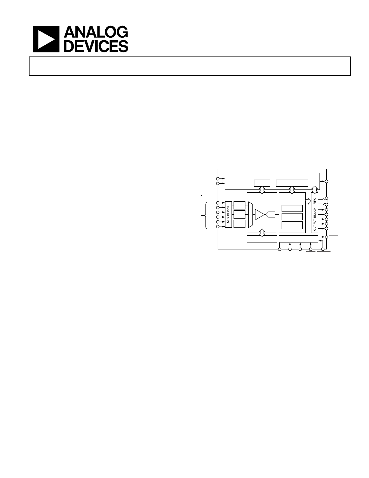
FUNCTIONAL BLOCK DIAGRAM
20B
XTAL1
XTAL
CLOCK PROCESSING BLOCK
PLL ADLLT PROCESSING
LLC
ANALOG
VIDEO
INPUTS
AIN1
AIN2
AIN3
AIN41
AIN51
AIN61
AA
FILTER
AA
FILTER
AA
FILTER
10-BIT, 86MHz
ADC
SHA A/D
DIGITAL
PROCESSING
BLOCK
2D COMB
VBI SLICER
COLOR
DEMOD
8-BIT/16-BIT2
PIXEL DATA
P15 TO P0
VS
HS
FIELD3
GPO5
SFL
ADV7180
REFERENCE
I2C/CONTROL
INTRQ
SCLK SDATA ALSB RESET PWRDWN4
1ONLY AVAILABLE ON 64-LEAD PACKAGE AND 48-LEAD PACKAGES.
216-BIT ONLY AVAILABLE ON 64-LEAD PACKAGE.
348-LEAD, 40-LEAD, AND 32-LEAD PACKAGE USES ONE LEAD FOR VS/FIELD.
4NOT AVAILABLE ON 32-LEAD PACKAGE.
5ONLY AVAILABLE ON 48-LEAD AND 64-LEAD PACKAGES.
Figure 1.
video performance for consumer applications with true 8-bit
data resolution. Three analog video input channels accept standard
composite, S-Video, or component video signals, supporting a
wide range of consumer video sources. AGC and clamp-restore
circuitry allow an input video signal peak-to-peak range to 1.0 V.
Alternatively, these can be bypassed for manual settings.
The line-locked clock output allows the output data rate, timing
signals, and output clock signals to be synchronous, asynchronous,
or line locked even with ±5% line length variation. Output
control signals allow glueless interface connections in many
applications. The ADV7180 is programmed via a 2-wire, serial
bidirectional port (I2C-compatible) and is fabricated in a 1.8 V
CMOS process. Its monolithic CMOS construction ensures greater
functionality with lower power dissipation. LFCSP package options
make the decoder ideal for space-constrained portable applications.
The 64-lead LQFP package is pin compatible with the ADV7181C.
1 The 48-Lead LQFP, 40-lead LFCSP, and 32-lead LFCSP use one pin to output
VS or FIELD.
One Technology Way, P.O. Box 9106, Norwood, MA 02062-9106, U.S.A.
Tel: 781.329.4700 ©2006-2015 Analog Devices, Inc. All rights reserved.
Technical Support
www.analog.com
1 page 
ADV7180
4/09—Rev. B to Rev. C
Changes to Features Section............................................................ 1
Changes to Absolute Maximum Ratings, Table 7....................... 11
Changes to Figure 7 and Table 8, EPAD Addition ..................... 12
Added Power-On RESET Section ................................................ 17
Changes to MAN_MUX_EN, Manual Input Muxing Enable,
Address 0xC4[7] Section and Table 12 ........................................ 17
Changes to Identification Section ................................................ 21
Added Table 16; Renumbered Sequentially ................................ 21
Changes to Table 21........................................................................ 23
Changes to CIL[2:0], Count Into Lock, Address 0x51[2:0]
Section and COL[2:0], Count Out of Lock, Address 0x51[5:3]
Section.............................................................................................. 25
Changes to Table 32 and Table 33 ................................................ 30
Changes to Table 34........................................................................ 32
Changes to Table 42........................................................................ 35
Changes to Table 52........................................................................ 38
Changes to Table 53 and Table 56 ................................................ 39
Changes to Table 61 and Figure 32............................................... 43
Added SQPE, Square Pixel Mode, Address 0x01[2] Section .... 44
Changes to NEWAVMODE, New AV Mode, Address 0x31[4]
Section.............................................................................................. 44
Changes to Figure 34...................................................................... 45
Changes to NFTOG[4:0], NTSC Field Toggle,
Address 0xE7[4:0] Section............................................................. 47
Changes to PFTOG, PAL Field Toggle, Address 0xEA[4:0]
Section.............................................................................................. 49
Changes to VDP Manuel Configuration Section ....................... 50
Changes to Table 66........................................................................ 51
Changes to Table 71........................................................................ 54
Changes to Table 72........................................................................ 55
Changes to VPS Section and PDC/UTC Section....................... 63
Changes to Gemstar_2x Format, Half-Byte Output Mode
Section.............................................................................................. 66
Changes to NTSC CCAP Data Section and PAL CCAP Data
Section.............................................................................................. 69
Changes to Figure 48...................................................................... 74
Changes to I2C Sequencer Section ............................................... 75
Changes to Table 102...................................................................... 76
Changes to Table 104...................................................................... 80
Changes to Table 105...................................................................... 97
Changes to Figure 53.................................................................... 108
Changes to Figure 54.................................................................... 109
Added Exposed Paddle Notation to Outline Dimensions ...... 110
Changes to Ordering Guide ........................................................ 111
Data Sheet
2/07—Rev. A to Rev. B
Changes to SFL_INV, Subcarrier Frequency Lock Inversion
Section.............................................................................................. 24
Changes to Table 103, Register 0x41............................................ 90
Updated Outline Dimensions..................................................... 111
11/06—Rev. 0 to Rev. A
Changes to Table 10 and Table 11 ................................................ 16
Changes to Table 30 ....................................................................... 28
Changes to Gain Operation Section ............................................ 33
Changes to Table 43 ....................................................................... 35
Changes to Table 97 ....................................................................... 72
Changes to Table 99 ....................................................................... 73
Changes to Table 103 ..................................................................... 80
Changes to Figure 54.................................................................... 110
1/06—Revision 0: Initial Version
Rev. J | Page 4 of 114
5 Page 
ADV7180
Data Sheet
TIMING SPECIFICATIONS
Guaranteed by characterization. AVDD = 1.71 V to 1.89 V, DVDD = 1.65 V to 2.0 V, DVDDIO = 1.62 V to 3.6 V, PVDD = 1.65 V to 2.0 V, specified
at operating temperature range, unless otherwise noted.
Table 5.
Parameter
SYSTEM CLOCK AND CRYSTAL
Nominal Frequency
Frequency Stability
I2C PORT
SCLK Frequency
SCLK Minimum Pulse Width High
SCLK Minimum Pulse Width Low
Hold Time (Start Condition)
Setup Time (Start Condition)
SDA Setup Time
SCLK and SDA Rise Times
SCLK and SDA Fall Times
Setup Time for Stop Condition
RESET FEATURE
Reset Pulse Width
CLOCK OUTPUTS
LLC Mark Space Ratio
DATA AND CONTROL OUTPUTS
Data Output Transitional Time
Data Output Transitional Time
Symbol Test Conditions
Min Typ
Max Unit
28.6363
±50
MHz
ppm
400 kHz
t1 0.6 µs
t2 1.3 µs
t3 0.6 µs
t4 0.6 µs
t5 100 ns
t6 300 ns
t7 300 ns
t8 0.6 µs
5 ms
t9:t10
45:55
55:45 % duty cycle
t11 Negative clock edge to start of valid data
(tSETUP = t10 − t11)
t12 End of valid data to negative clock edge
(tHOLD = t9 − t12)
3.6 ns
2.4 ns
Timing Diagrams
SDATA
SCLK
t3 t5
t6
t2
t1
t7
Figure 6. I2C Timing
t3
t4
t8
OUTPUT LLC
t9 t10
OUTPUTS P0 TO P7, HS,
VS/FIELD/SFL
t11
t12
Figure 7. Pixel Port and Control Output Timing
Rev. J | Page 10 of 114
11 Page | ||
| Páginas | Total 30 Páginas | |
| PDF Descargar | [ Datasheet ADV7180.PDF ] | |
Hoja de datos destacado
| Número de pieza | Descripción | Fabricantes |
| ADV7180 | 4 x Oversampling SDTV Video Decoder | Analog Devices |
| ADV7181 | Multiformat SDTV Video Decoder | Analog Devices |
| ADV7181B | Multiformat SDTV Video Decoder | Analog Devices |
| ADV7183A | Multiformat SDTV Video Decoder | Analog Devices |
| Número de pieza | Descripción | Fabricantes |
| SLA6805M | High Voltage 3 phase Motor Driver IC. |
Sanken |
| SDC1742 | 12- and 14-Bit Hybrid Synchro / Resolver-to-Digital Converters. |
Analog Devices |
|
DataSheet.es es una pagina web que funciona como un repositorio de manuales o hoja de datos de muchos de los productos más populares, |
| DataSheet.es | 2020 | Privacy Policy | Contacto | Buscar |