|
|
|
PDF AD7327 Data sheet ( Hoja de datos )
| Número de pieza | AD7327 | |
| Descripción | 12-Bit Plus Sign ADC | |
| Fabricantes | Analog Devices | |
| Logotipo | ||
Hay una vista previa y un enlace de descarga de AD7327 (archivo pdf) en la parte inferior de esta página. Total 30 Páginas | ||
|
No Preview Available !
www.DataSheet4U.com
500 kSPS, 8-Channel, Software-Selectable,
True Bipolar Input, 12-Bit Plus Sign ADC
AD7327
FEATURES
12-bit plus sign SAR ADC
True bipolar input ranges
Software-selectable input ranges
±10 V, ±5 V, ±2.5 V, 0 V to +10 V
500 kSPS throughput rate
Eight analog input channels with channel sequencer
Single-ended, true differential, and pseudo differential
analog input capability
High analog input impedance
Low power: 17 mW
Temperature indicator
Full power signal bandwidth: 22 MHz
Internal 2.5 V reference
High speed serial interface
Power-down modes
20-lead TSSOP package
iCMOS™ process technology
GENERAL DESCRIPTION
The AD73271 is an 8-channel, 12-bit plus sign successive
approximation ADC designed on the iCMOS (industrial
CMOS) process. iCMOS is a process combining high voltage
silicon with submicron CMOS and complementary bipolar
technologies. It enables the development of a wide range of high
performance analog ICs capable of 33 V operation in a footprint
that no previous generation of high voltage parts could achieve.
Unlike analog ICs using conventional CMOS processes, iCMOS
components can accept bipolar input signals while providing
increased performance, dramatically reduced power
consumption, and reduced package size.
The AD7327 can accept true bipolar analog input signals. The
AD7327 has four software-selectable input ranges, ±10 V, ±5 V,
±2.5 V, and 0 V to +10 V. Each analog input channel can be
independently programmed to one of the four input ranges.
The analog input channels on the AD7327 can be programmed
to be single-ended, true differential, or pseudo differential.
The ADC contains a 2.5 V internal reference. The AD7327 also
allows for external reference operation. If a 3 V reference is
applied to the REFIN/OUT pin, the AD7327 can accept a true
bipolar ±12 V analog input. Minimum ±12 V VDD and VSS
supplies are required for the ±12 V input range. The ADC has a
high speed serial interface that can operate at throughput rates
up to 500 kSPS.
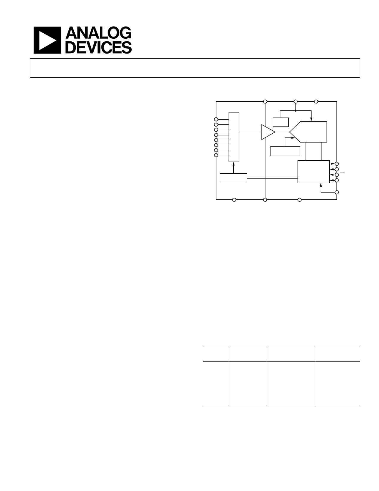
FUNCTIONAL BLOCK DIAGRAM
VDD
REFIN/OUT VCC
AD7327
VIN0
VIN1
VIN2
VIN3
VIN4
VIN5
VIN6
VIN7
I/P
MUX
2.5V
VREF
T/H
13-BIT
SUCCESSIVE
APPROXIMATION
ADC
TEMPERATURE
INDICATOR
CHANNEL
SEQUENCER
CONTROL LOGIC
AND REGISTERS
AGND
VSS DGND
Figure 1.
DOUT
SCLK
CS
DIN
VDRIVE
PRODUCT HIGHLIGHTS
1. The AD7327 can accept true bipolar analog input signals,
±10 V, ±5 V, ±2.5 V, and 0 V to +10 V unipolar signals.
2. The eight analog inputs can be configured as eight single-
ended inputs, four true differential inputs, four pseudo
differential inputs, or seven pseudo differential inputs.
3. 500 kSPS serial interface. SPI®-/QSPI™-/DSP-/MICROWIRE™-
compatible interface.
4. Low power, 17 mW, at a maximum throughput rate of
500 kSPS.
5. Channel sequencer.
Table 1. Similar Devices
Device Throughput
Number Rate
AD7329 1000 kSPS
AD7328 1000 kSPS
AD7324 1000 kSPS
AD7323 500 kSPS
AD7322 1000 kSPS
AD7321 500 kSPS
Number of bits
12-bit plus sign
12-bit plus sign
12-bit plus sign
12-bit plus sign
12-bit plus sign
12-bit plus sign
Number of
Channels
8
8
4
4
2
2
1 Protected by U.S. Patent No. 6,731,232.
Rev. 0
Information furnished by Analog Devices is believed to be accurate and reliable. However, no
responsibility is assumed by Analog Devices for its use, nor for any infringements of patents or other
rights of third parties that may result from its use. Specifications subject to change without notice. No
license is granted by implication or otherwise under any patent or patent rights of Analog Devices.
Trademarksandregisteredtrademarksarethepropertyoftheirrespectiveowners.
One Technology Way, P.O. Box 9106, Norwood, MA 02062-9106, U.S.A.
Tel: 781.329.4700
www.analog.com
Fax: 781.461.3113
©2006 Analog Devices, Inc. All rights reserved.
1 page 
Parameter1
ANALOG INPUT
Input Voltage Ranges
(Programmed via Range
Registers)
Pseudo Differential VIN(−)
Input Range
DC Leakage Current
Input Capacitance3
REFERENCE INPUT/OUTPUT
Input Voltage Range
Input DC Leakage Current
Input Capacitance
Reference Output Voltage
Reference Output Voltage Error
@ 25°C
Reference Output Voltage
TMIN to TMAX
Reference Temperature
Coefficient
Reference Output Impedance
LOGIC INPUTS
Input High Voltage, VINH
Input Low Voltage, VINL
Input Current, IIN
Input Capacitance, CIN3
LOGIC OUTPUTS
Output High Voltage, VOH
Output Low Voltage, VOL
Floating-State Leakage Current
Floating-State Output
Capacitance3
Output Coding
CONVERSION RATE
Conversion Time
Track-and-Hold Acquisition
Time2, 3
Throughput Rate
B Version
Min Typ Max
±10
±5
±2.5
0 to 10
±3.5
±6
±5
+3/−5
3
13.5
16.5
21.5
3
±80
2.5 3
±1
10
2.5
±5
±10
25
3
7
2.4
10
0.8
0.4
±1
VDRIVE −
0.2 V
5
0.4
±1
Straight natural binary
Twos complement
1.6
305
500
AD7327
Unit Test Conditions/Comments
Reference = 2.5 V; see Table 6
V VDD = 10 V min, VSS = −10 V min, VCC = 2.7 V to 5.25 V
V VDD = 5 V min, VSS = −5 V min, VCC = 2.7 V to 5.25 V
V VDD = 5 V min, VSS = −5 V min, VCC = 2.7 V to 5.25 V
V VDD = 10 V min, VSS = AGND min, VCC = 2.7 V to 5.25 V
VDD = 16.5 V, VSS = −16.5 V, VCC = 5 V; see Figure 40 and
Figure 41
V Reference = 2.5 V; range = ±10 V
V Reference = 2.5 V; range = ±5 V
V Reference = 2.5 V; range = ±2.5 V
V Reference = 2.5 V; range = 0 V to +10 V
nA VIN = VDD or VSS
nA Per input channel, VIN = VDD or VSS
pF When in track, ±10 V range
pF When in track, ±5 V and 0 V to +10 V ranges
pF When in track, ±2.5 V range
pF When in hold, all ranges
V
μA
pF
V
mV
mV
ppm/°C
ppm/°C
Ω
V
V VCC = 4.75 V to 5.25 V
V VCC = 2.7 to 3.6 V
μA VIN = 0 V or VDRIVE
pF
V ISOURCE = 200 μA
V ISINK = 200 μA
μA
pF
Coding bit set to 1 in control register
Coding bit set to 0 in control register
μs
ns
kSPS
16 SCLK cycles with SCLK = 10 MHz
Full-scale step input; see the Terminology section
See the Serial Interface section
Rev. 0 | Page 5 of 36
5 Page 
–50
VCC = VDRIVE = 3V
–55 VDD/VSS = ±12V
TA = 25°C
–60 fS = 500kSPS
INTERNAL REFERENCE
–65
–70
–75
–80
–85
–90
–95
0V TO +10V SE
±10V SE
±10V DIFF
0V TO +10V DIFF
±5V SE
±5V DIFF
±2.5V DIFF
±2.5V SE
–100
10
100 1000
ANALOG INPUT FREQUENCY (kHz)
Figure 10. THD vs. Analog Input Frequency
for Single-Ended (SE) and True Differential Mode (Diff) at 3 V VCC
–50
VCC = VDRIVE = 5V
–55 VDD/VSS = ±12V
TA = 25°C
–60 fS = 500kSPS
INTERNAL REFERENCE
–65
–70
0V TO +10V SE
±10V SE
±10V DIFF
–75
–80
–85
–90
–95
–100
10
0V TO +10V DIFF
±5V SE
±5V DIFF
±2.5V SE
±2.5V DIFF
100
ANALOG INPUT FREQUENCY (kHz)
1000
Figure 11. THD vs. Analog Input Frequency
for Single-Ended (SE) and True Differential Mode (Diff) at 5 V VCC
80
±5V DIFF
±2.5V DIFF
75 ±5V SE
±2.5V SE
0V TO +10V DIFF
70 ±10V DIFF
±10V SE
65
0V TO +10V SE
60
55
50
10
VCC = VDRIVE = 3V
VDD/VSS = ±12V
TA = 25°C
fS = 500kSPS
INTERNAL REFERENCE
100
ANALOG INPUT FREQUENCY (kHz)
1000
Figure 12. SINAD vs. Analog Input Frequency
for Single-Ended (SE) and True Differential Mode (Diff) at 3 V VCC
AD7327
80
±5V DIFF
±2.5V DIFF
75
±5V SE
±2.5V SE
70 ±10V DIFF
65
±10V SE
0V TO +10V DIFF
0V TO +10V SE
60
55
50
10
VCC = VDRIVE = 5V
VDD/VSS = ±12V
TA = 25°C
fS = 500kSPS
INTERNAL REFERENCE
100 1000
ANALOG INPUT FREQUENCY (kHz)
Figure 13. SINAD vs. Analog Input Frequency
for Single-Ended (SE) and True Differential Mode (Diff) at 5 V VCC
–50
–55
–60
–65
–70
–75
–80
–85
–90
–95
0
VCC = 3V
VCC = 5V
VDD/VSS = ±12V
SINGLE-ENDED MODE
fS = 500kSPS
TA = 25°C
50kHz ON SELECTED CHANNEL
100 200 300 400 500
FREQUENCY OF INPUT NOISE (kHz)
Figure 14. Channel-to-Channel Isolation
600
10k
9469
VCC = 5V
9k VDD/VSS = ±12V
RANGE = ±10V
8k 10k SAMPLES
TA = 25°C
7k
6k
5k
4k
3k
2k
1k
0 228
303 0
0
–2 –1
0
1
2
CODE
Figure 15. Histogram of Codes, True Differential Mode
Rev. 0 | Page 11 of 36
11 Page | ||
| Páginas | Total 30 Páginas | |
| PDF Descargar | [ Datasheet AD7327.PDF ] | |
Hoja de datos destacado
| Número de pieza | Descripción | Fabricantes |
| AD7321 | 12-Bit Plus Sign ADC | Analog Devices |
| AD7322 | 12-Bit Plus Sign ADC | Analog Devices |
| AD7323 | 12-Bit Plus Sign ADC | Analog Devices |
| AD7324 | 12-Bit Plus Sign ADC | Analog Devices |
| Número de pieza | Descripción | Fabricantes |
| SLA6805M | High Voltage 3 phase Motor Driver IC. |
Sanken |
| SDC1742 | 12- and 14-Bit Hybrid Synchro / Resolver-to-Digital Converters. |
Analog Devices |
|
DataSheet.es es una pagina web que funciona como un repositorio de manuales o hoja de datos de muchos de los productos más populares, |
| DataSheet.es | 2020 | Privacy Policy | Contacto | Buscar |