|
|
|
PDF NIF5003N Data sheet ( Hoja de datos )
| Número de pieza | NIF5003N | |
| Descripción | Self-Protected FET | |
| Fabricantes | ON Semiconductor | |
| Logotipo | ||
Hay una vista previa y un enlace de descarga de NIF5003N (archivo pdf) en la parte inferior de esta página. Total 5 Páginas | ||
|
No Preview Available !
www.DataSheet4U.com
NIF5003N
Preferred Device
Self−Protected FET
with Temperature and
Current Limit
42 V, 14 A, Single N−Channel, SOT−223
HDPlus™ devices are an advanced series of power MOSFETs which
utilize ON Semiconductors latest MOSFET technology process to
achieve the lowest possible on−resistance per silicon area while
incorporating smart features. Integrated thermal and current limits
work together to provide short circuit protection. The devices feature
an integrated Drain−to−Gate Clamp that enables them to withstand
high energy in the avalanche mode. The Clamp also provides
additional safety margin against unexpected voltage transients.
Electrostatic Discharge (ESD) protection is provided by an integrated
Gate−to−Source Clamp.
Features
• Short Circuit Protection/Current Limit
• Thermal Shutdown with Automatic Restart
• IDSS Specified at Elevated Temperature
• Avalanche Energy Specified
• Slew Rate Control for Low Noise Switching
• Overvoltage Clamped Protection
• Pb−Free Packages are Available
http://onsemi.com
VDSS
(Clamped)
42 V
RDS(on) TYP
53 mW @ 10 V
ID MAX
(Limited)
14 A
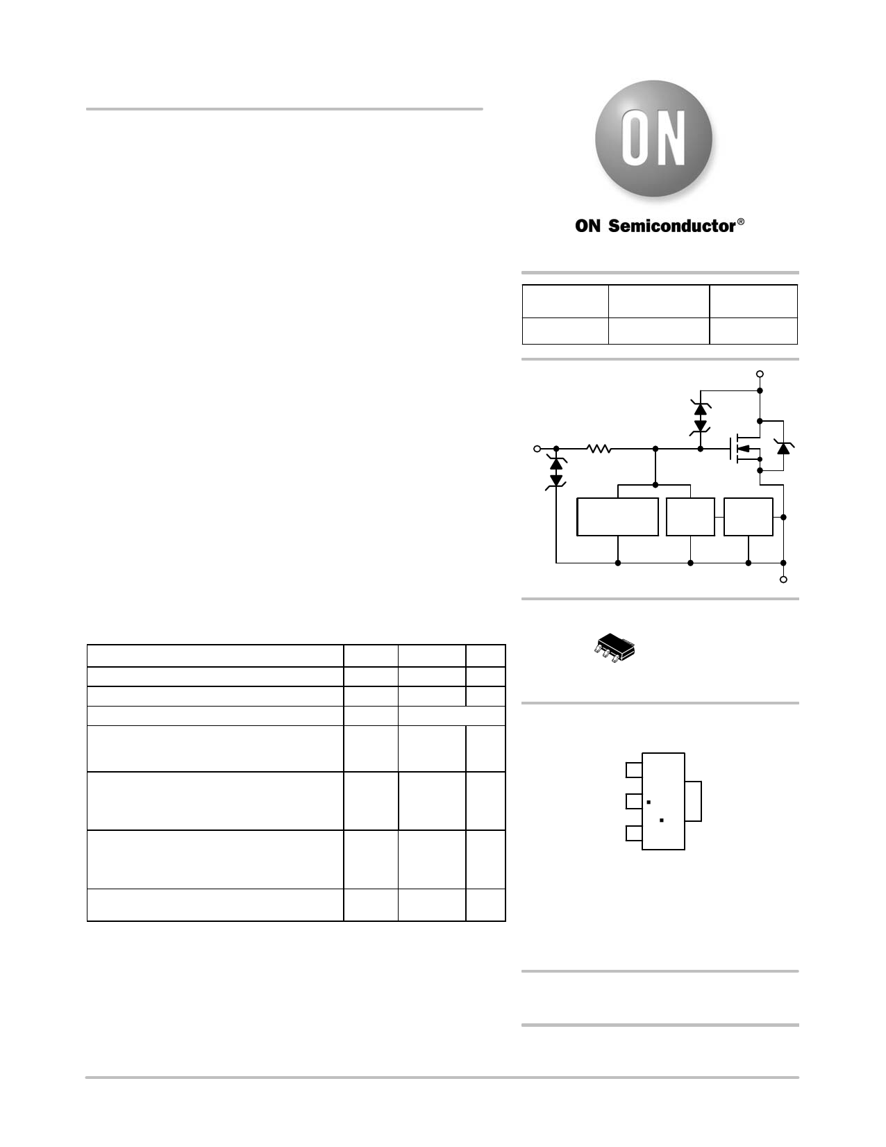
Drain
Gate
Input
Overvoltage
Protection
RG
MPWR
ESD Protection
Temperature Current Current
Limit
Limit Sense
Source
MAXIMUM RATINGS (TJ = 25°C unless otherwise noted)
Rating
Symbol Value Unit
Drain−to−Source Voltage Internally Clamped
Gate−to−Source Voltage
Drain Current
Continuous
Total Power Dissipation
@ TA = 25°C (Note 1)
@ TA = 25°C (Note 2)
Thermal Resistance
Junction−to−Case
Junction−to−Ambient (Note 1)
Junction−to−Ambient (Note 2)
Single Pulse Drain−to−Source Avalanche Energy
(VDD = 25 Vdc, VGS = 5.0 Vdc,
VDS = 40 Vdc, IL = 3.2 Apk, L = 120 mH,
RG = 25 W)
Operating and Storage Temperature Range
(Note 3)
VDSS
VGS
ID
PD
RqJC
RqJA
RqJA
EAS
42 Vdc
"14
Vdc
Internally Limited
W
1.25
1.9
°C/W
12
100
65
400 mJ
TJ, Tstg −55 to 150 °C
Stresses exceeding Maximum Ratings may damage the device. Maximum Ratings
are stress ratings only. Functional operation above the Recommended Operating
Conditions is not implied. Extended exposure to stresses above the Recommended
Operating Conditions may affect device reliability.
1. Surface mounted onto minimum pad size (0.412″ square) FR4 PCB, 1 oz cu.
2. Mounted onto 1″ square pad size (1.127″ square) FR4 PCB, 1 oz cu.
3. Normal pre−fault operating range. See thermal limit range conditions.
4
1
2
3
SOT−223
CASE 318E
STYLE 3
MARKING DIAGRAM
GATE
DRAIN
SOURCE
1
2
3
4
DRAIN
A = Assembly Location
Y = Year
W = Work Week
5003N = Specific Device Code
G = Pb−Free Package
(Note: Microdot may be in either location)
ORDERING INFORMATION
See detailed ordering and shipping information in the package
dimensions section on page 4 of this data sheet.
Preferred devices are recommended choices for future use
and best overall value.
© Semiconductor Components Industries, LLC, 2006
April, 2006 − Rev. 2
1
Publication Order Number:
NIF5003N/D
1 page 
NIF5003N
PACKAGE DIMENSIONS
D
b1
4
HE
1 23
E
e1
e
0.08 (0003)
A1
b
A
SOT−223 (TO−261)
CASE 318E−04
ISSUE L
NOTES:
1. DIMENSIONING AND TOLERANCING PER ANSI
Y14.5M, 1982.
2. CONTROLLING DIMENSION: INCH.
MILLIMETERS
INCHES
DIM MIN NOM MAX
MIN NOM MAX
A 1.50
1.63
1.75
0.060 0.064 0.068
A1 0.02
0.06
0.10
0.001 0.002 0.004
b 0.60 0.75 0.89 0.024 0.030 0.035
b1 2.90
3.06
3.20
0.115 0.121 0.126
c 0.24 0.29 0.35 0.009 0.012 0.014
D 6.30
6.50
6.70
0.249 0.256 0.263
E 3.30
3.50
3.70
0.130 0.138 0.145
e 2.20 2.30 2.40 0.087 0.091 0.094
e1 0.85
0.94
1.05
0.033 0.037 0.041
L1 1.50
1.75
2.00
0.060 0.069 0.078
C
H E 6.70
7.00
7.30
0.264 0.276 0.287
q q 0° − 10° 0° − 10°
STYLE 3:
PIN 1. GATE
L1
2. DRAIN
3. SOURCE
4. DRAIN
SOLDERING FOOTPRINT*
3.8
0.15
2.0
0.079
2.3
0.091
2.3
0.091
6.3
0.248
2.0
0.079
1.5
0.059
ǒ ǓSCALE 6:1
mm
inches
*For additional information on our Pb−Free strategy and soldering
details, please download the ON Semiconductor Soldering and
Mounting Techniques Reference Manual, SOLDERRM/D.
HDPlus is a trademark of Semiconductor Components Industries, LLC (SCILLC)
ON Semiconductor and
are registered trademarks of Semiconductor Components Industries, LLC (SCILLC). SCILLC reserves the right to make changes without further notice
to any products herein. SCILLC makes no warranty, representation or guarantee regarding the suitability of its products for any particular purpose, nor does SCILLC assume any liability
arising out of the application or use of any product or circuit, and specifically disclaims any and all liability, including without limitation special, consequential or incidental damages.
“Typical” parameters which may be provided in SCILLC data sheets and/or specifications can and do vary in different applications and actual performance may vary over time. All
operating parameters, including “Typicals” must be validated for each customer application by customer’s technical experts. SCILLC does not convey any license under its patent rights
nor the rights of others. SCILLC products are not designed, intended, or authorized for use as components in systems intended for surgical implant into the body, or other applications
intended to support or sustain life, or for any other application in which the failure of the SCILLC product could create a situation where personal injury or death may occur. Should
Buyer purchase or use SCILLC products for any such unintended or unauthorized application, Buyer shall indemnify and hold SCILLC and its officers, employees, subsidiaries, affiliates,
and distributors harmless against all claims, costs, damages, and expenses, and reasonable attorney fees arising out of, directly or indirectly, any claim of personal injury or death
associated with such unintended or unauthorized use, even if such claim alleges that SCILLC was negligent regarding the design or manufacture of the part. SCILLC is an Equal
Opportunity/Affirmative Action Employer. This literature is subject to all applicable copyright laws and is not for resale in any manner.
PUBLICATION ORDERING INFORMATION
LITERATURE FULFILLMENT:
Literature Distribution Center for ON Semiconductor
P.O. Box 61312, Phoenix, Arizona 85082−1312 USA
Phone: 480−829−7710 or 800−344−3860 Toll Free USA/Canada
Fax: 480−829−7709 or 800−344−3867 Toll Free USA/Canada
Email: [email protected]
N. American Technical Support: 800−282−9855 Toll Free
USA/Canada
Japan: ON Semiconductor, Japan Customer Focus Center
2−9−1 Kamimeguro, Meguro−ku, Tokyo, Japan 153−0051
Phone: 81−3−5773−3850
http://onsemi.com
5
ON Semiconductor Website: http://onsemi.com
Order Literature: http://www.onsemi.com/litorder
For additional information, please contact your
local Sales Representative.
NIF5003N/D
5 Page | ||
| Páginas | Total 5 Páginas | |
| PDF Descargar | [ Datasheet NIF5003N.PDF ] | |
Hoja de datos destacado
| Número de pieza | Descripción | Fabricantes |
| NIF5003N | Self-Protected FET | ON Semiconductor |
| Número de pieza | Descripción | Fabricantes |
| SLA6805M | High Voltage 3 phase Motor Driver IC. |
Sanken |
| SDC1742 | 12- and 14-Bit Hybrid Synchro / Resolver-to-Digital Converters. |
Analog Devices |
|
DataSheet.es es una pagina web que funciona como un repositorio de manuales o hoja de datos de muchos de los productos más populares, |
| DataSheet.es | 2020 | Privacy Policy | Contacto | Buscar |