|
|
|
PDF CDB61584A Data sheet ( Hoja de datos )
| Número de pieza | CDB61584A | |
| Descripción | Dual Line Interface Unit | |
| Fabricantes | Cirrus Logic | |
| Logotipo | ||
Hay una vista previa y un enlace de descarga de CDB61584A (archivo pdf) en la parte inferior de esta página. Total 12 Páginas | ||
|
No Preview Available !
www.DataSheet4U.com
CDB61584A
Product Databook
FEATURES
s Socketed CS61584A Dual Line Interface
s All Required Components for CS61584A
Evaluation
s Locations to Evaluate Protection Circuitry
s LED Status Indications for Alarm Conditions
s Support for Hardware and Host Modes
Dual Line
Interface Unit
DESCRIPTION
The evaluation board includes a socketed CS61584A
dual line interface device and all support components
necessary for evaluation. The board is powered by an
external +5 Volt supply.
ORDERING INFORMATION:
CDB61584A
The board may be configured for 100Ω twisted-pair T1,
75Ω coax E1, or 120Ω twisted-pair E1 operation. Bind-
ing posts and bantam jacks are provided for line
interface connections. Several BNC connectors provide
clock and data I/O at the system interface. Reference
timing may be derived from a quartz crystal, crystal os-
cillator, or an external reference clock. Four LED
indicators monitor device alarm conditions.
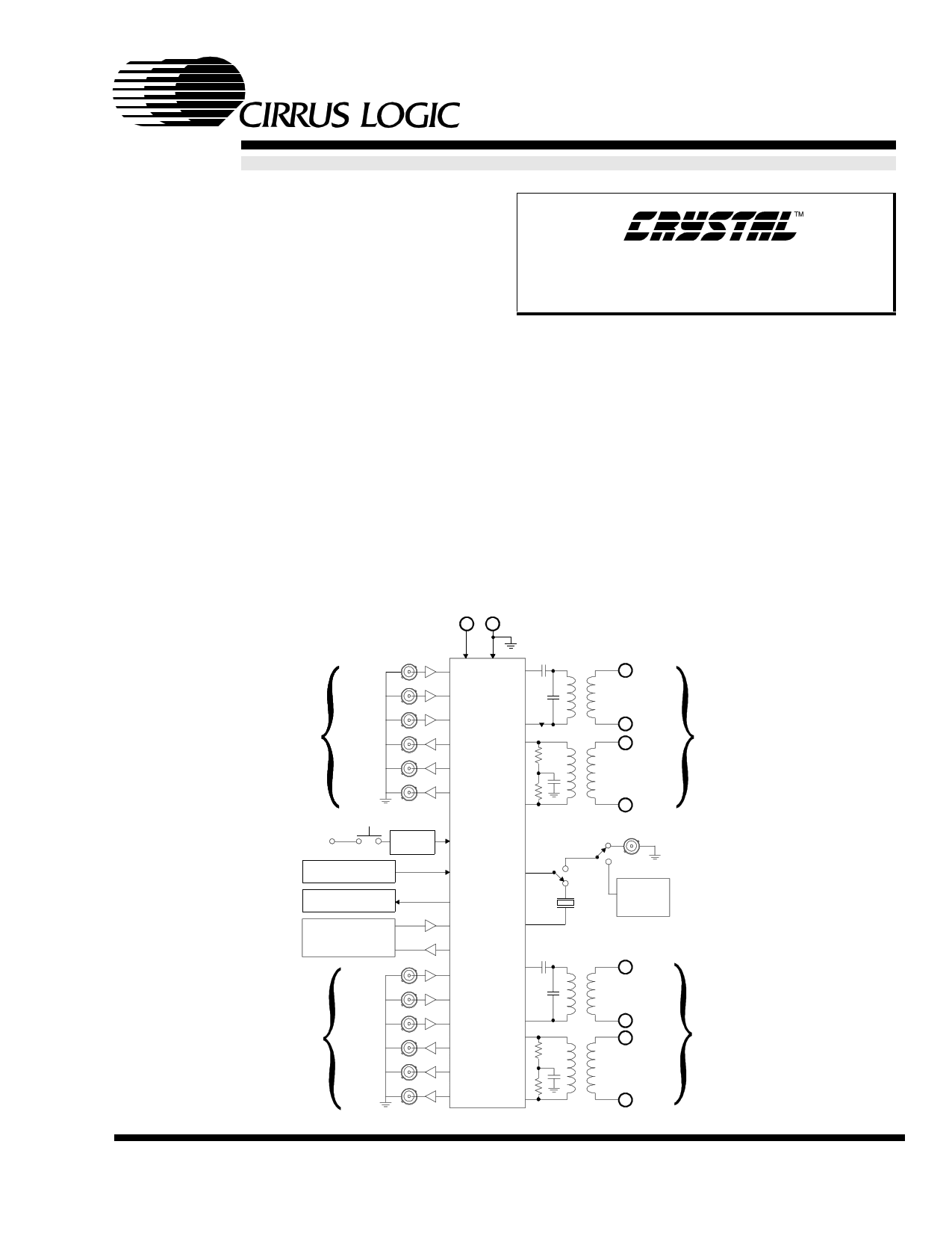
5V+ 0V
DS261DB2
CHANNEL 1
TCLK1
TPOS1
(TDATA1)
TNEG1
RCLK1
RPOS1
(RDATA1)
RNEG1
(BPV1)
V+
RESET
CIRCUIT
Hardware Control
and Mode Circuit
LED Status
Indicators
Serial Interface
Control Circuit
CHANNEL 2
TCLK2
TPOS2
(TDATA2)
TNEG2
RCLK2
RPOS2
(RDATA2)
RNEG2
(BPV2)
CS61584A
TTIP1
TRING1
RTIP1
CHANNEL 1
RRING1
REFCLK
Oscillator
XTL Circuit
TTIP2
TRING2
RTIP2
CHANNEL 2
RRING2
Copyright © Cirrus Logic, Inc. 1998
(All Rights Reserved)
MAR ‘98
1 page 
CDB61584A
Dual Line Interface Unit
EVALUATION HINTS
1) The orientation of pin 1 for the CS61584A is la-
beled "1" on the left side of the socket U7.
2) A jumper must not be placed on header J10
when using the CDB61584A.
3) Component locations R3-R4, R14-R15, C1,
and C12 must have the correct values installed
according to the application. All the necessary
components are included with the evaluation
board.
4) Closing a DIP switch on SW2, SW3, and SW4
towards the label sets the CS61584A control
pin of the same name to logic 1.
5) When performing a manual loopback of the re-
covered signal to the transmit signal at the BNC
connectors, the recovered data must be valid on
the falling edge of RCLK to properly latch the
data in the transmit direction. To accomplish
this, the SW2 switch position labeled "CLKE"
must be closed (logic 1) during Hardware mode
operation or the CLKE bit in the Control A reg-
ister must be set to a 1 during Host mode oper-
ation.
6) Jumpers can be placed on headers J9 and J12 to
provide a ground reference on TRING for 75Ω
coax E1 applications.
7) Properly terminate TTIP/TRING when evalu-
ating the transmit output pulse shape. For more
information concerning pulse shape evaluation,
refer to the Crystal application note entitled
"Measurement and Evaluation of Pulse Shapes
in T1/E1 Transmission Systems."
DS261DB2
55
5 Page 
• Notes •
11 Page | ||
| Páginas | Total 12 Páginas | |
| PDF Descargar | [ Datasheet CDB61584A.PDF ] | |
Hoja de datos destacado
| Número de pieza | Descripción | Fabricantes |
| CDB61584A | Dual Line Interface Unit | Cirrus Logic |
| Número de pieza | Descripción | Fabricantes |
| SLA6805M | High Voltage 3 phase Motor Driver IC. |
Sanken |
| SDC1742 | 12- and 14-Bit Hybrid Synchro / Resolver-to-Digital Converters. |
Analog Devices |
|
DataSheet.es es una pagina web que funciona como un repositorio de manuales o hoja de datos de muchos de los productos más populares, |
| DataSheet.es | 2020 | Privacy Policy | Contacto | Buscar |