|
|
|
PDF A8290 Data sheet ( Hoja de datos )
| Número de pieza | A8290 | |
| Descripción | Single LNB Supply and Control Voltage Regulator | |
| Fabricantes | Allegro MicroSystems | |
| Logotipo | ||
Hay una vista previa y un enlace de descarga de A8290 (archivo pdf) en la parte inferior de esta página. Total 19 Páginas | ||
|
No Preview Available !
www.DataSheet4U.com
A8290
Single LNB Supply and Control Voltage Regulator
Features and Benefits
▪ 2-wire serial I2C™ -compatible interface: control (write) and
status (read)
▪ LNB voltages (16 programmable levels) compatible with
all common standards
▪ Tracking switch-mode power converter for lowest dissipation
▪ Integrated converter switches and current sensing
▪ Provides up to 650 mA continuous load current
▪ Provides up to 700 mA of current for 2000 ms
▪ Output current limit of 900 mA typical, with 48 ms timer
▪ Static current limit circuit allows full current at startup and
13→18V output transition; reliably starts wide load range
▪ Push-pull output stage minimizes 13→18V and 18→13V
output transition times for highly capacitive loads
▪ Adjustable rise/fall time via external timing capacitor
▪ Built-in tone oscillator, factory-trimmed to 22 kHz
facilitates DiSEqC™ tone encoding, even at no-load
▪ Four methods of 22 kHz tone generation, via I2C™ data
bits and/or external pin
▪ Filter bypass MOSFET minimizes losses during tone transmit
▪ 22 kHz tone detector facilitates DiSEqC™ 2.0 decoding
▪ Provides VOUT within 19 to 21 VDC at 700 mA for
SWM (single wire multiswitch) operation
▪ Diagnostics for output voltage level, input supply UVLO,
and DiSEqC™ tone output
▪ Auxiliary modulation input
▪ LNB overcurrent with timer
▪ Cable disconnect diagnostic
Package:
28 pin 5 mm × 5mm MLP/QFN
(suffix ET)
Description
Intended for analog and digital satellite receivers, this single
low noise block converter regulator (LNBR) is a monolithic
linear and switching voltage regulator, specifically designed to
provide the power and the interface signals to an LNB down
converter via coaxial cable. The A8290 requires few external
components, with the boost switch and compensation circuitry
integrated inside of the device. A high switching frequency is
chosen to minimize the size of the passive filtering components,
further assisting in cost reduction.The high levels of component
integration ensure extremely low noise and ripple figures.
The A8290 has been designed for high efficiency, utilizing
the Allegro® advanced BCD process. The integrated boost
switch has been optimized to minimize both switching and
static losses. To further enhance efficiency, the voltage drop
across the tracking regulator has been minimized.
The A8290 has integrated tone detection capability, to support
full two-way DiSEqC™ communications. Several schemes
are available for generating tone signals, all the way down to
no-load, and using either the internal clock or an external time
source. A DiSEqC™ filter bypass switch is also integrated, to
minimize the output impedance during tone generation.
Continued on the next page…
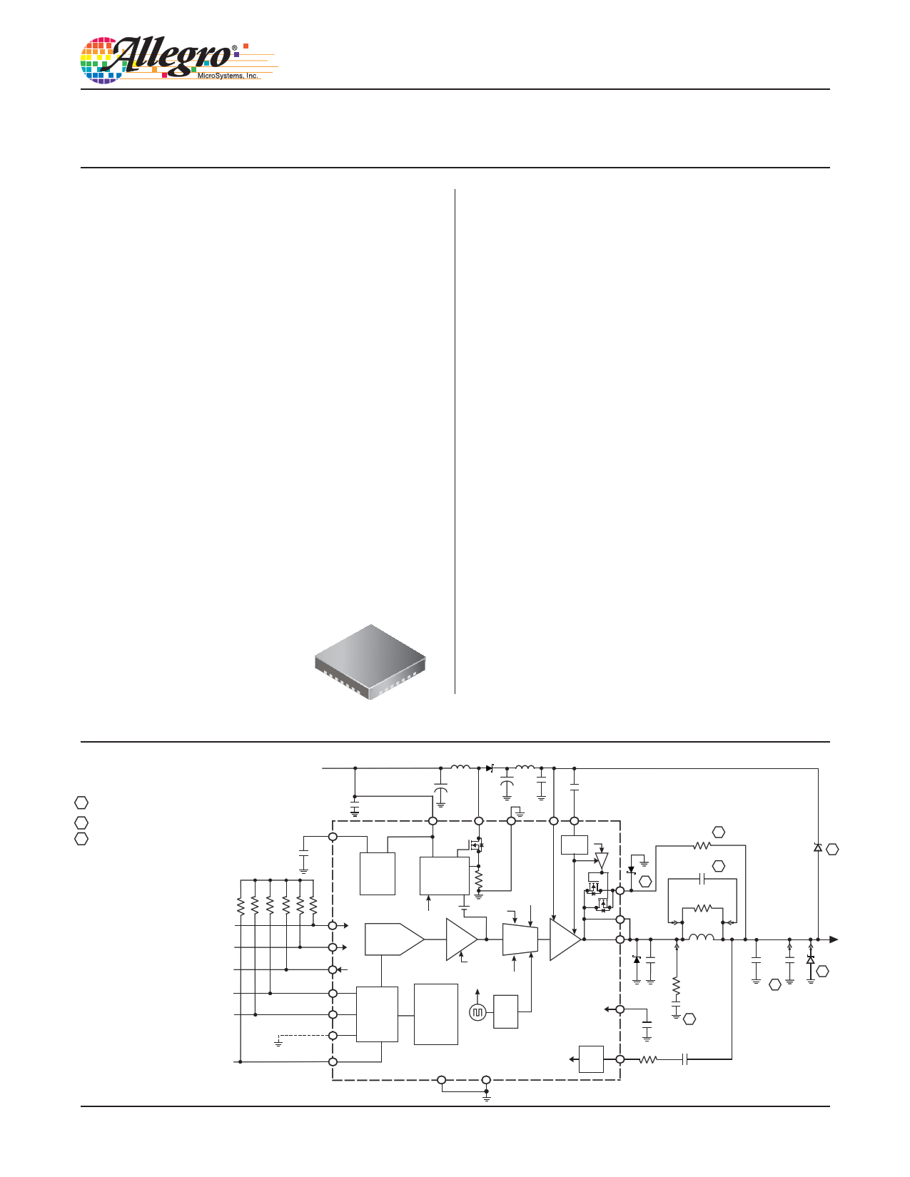
Functional Block Diagram VS
A
R9-C11 network is needed only when a highly
inductive load is applied, such as ProBand LNB.
B D2, D4, D5, and R10 are used for surge protection.
C Either C12 or C9 should be used, but not both.
VDD
VREG
C3
220 nF
R1 R2 R3 R4 R5 R6
EXTM
BFC
TDO
SDA
SCL
ADD
IRQ
C1
100 nF
Regulator
DAC
I2 C™-
Compatible
Interface
C2
100 μF
L1
33 μH
D1
L3
1 MH
C5 C6
100 μF 0.68 μF
C4
100 nF
VIN
LX GNDLX
BOOST VCP
Boost
Converter
Charge BFC
Pump
VPump
fsw
LNB
Voltage
Control
EXTM
TMode
Wave
Shape
Linear
Stage
TCAP
Fault Monitor
TGate
fsw
OCP
PNG
TSD
VUV
Clock
Divider 22 kHz
Oscillator
D2
B
BFO
BFI
R10 B
17
C12 C
R7
15 7
LNB
C8
D3 220 nF
TCAP
C7
10 nF
L2
220 μH
R9
30 7
C11
0.68 μF
A
C13
10 nF
C9
220 nF
C
PAD
GND
TDO
Tone
Detect
TDI R8
100 7
C10
10 nF
D5
B
VOUT
D4
B
8290-DS, Rev.2
1 page 
A8290
Single LNB Supply and Control Voltage Regulator
ELECTRICAL CHARACTERISTICS (continued) at TA = 25°C, VIN = 8 to 16 V, unless noted otherwise1
Characteristics
Symbol
Test Conditions
Min.
Bypass FET
Bypass FET Control (BFC) Logic Input
Input Leakage
Bypass FET On Resistance
VBFC(H)
VBFC(L)
IBFCLKG
RDS(on)
ILOAD = 500 mA, and VBFC = Low, or
BFC2 bit = 1
2.0
–
–1
–
Turn On/Off Delay2
Tone
tD(ON/OFF) VBFC = Low, or BFC2 bit = 1
–
Tone Frequency
Tone Amplitude, Peak-to-Peak
Tone Duty Cycle
Tone Rise Time
Tone Fall Time
EXTM Logic Input
EXTM Input Leakage
Tone Detector
fTONE
VTONE(pp)
DCTONE
trTONE
tfTONE
VEXTM(H)
VEXTM(L)
IEXTMLKG
ILOAD = 0 to 500 mA, CLOAD = 750 nF
ILOAD = 0 to 500 mA, CLOAD = 750 nF
ILOAD = 0 to 500 mA, CLOAD = 750 nF
ILOAD = 0 to 500 mA, CLOAD = 750 nF
20
400
40
5
5
2.0
–
–1
Tone Detect Input Amplitude Receive, Peak-to-Peak
Tone Detect Input Amplitude Transmit, Peak-
to-Peak
VTDR(pp)
VTDT(pp)Int
VTDT(pp)Ext
fTONE = 22 kHz sine wave, TMODE = 0
fTONE = 22 kHz sine wave, using internal tone
(options 1 and 2, in figure 2)
fTONE = 22 kHz sine wave, using external
tone (options 3 and 4, in figure 2)
300
400
300
Tone Reject Input Amplitude, Peak-to-Peak
Frequency Capture
Input Impedance2
TDO Output Voltage
TDO Output Leakage
I2C™-Compatible Interface
VTRI(pp)
fTDI
ZTDI
VTDO(L)
ITDOLKG
fTONE = 22 kHz sine wave
600 mVpp sine wave
Tone present, ILOAD = 3 mA
Tone absent, VTDO = 7 V
–
17.6
–
–
–
Logic Input (SDA, SCL) Low Level
Logic Input (SDA, SCL) High Level
Logic Input Hysteresis
Logic Input Current
Logic Output Voltage SDA and IRQ
Logic Output Leakage SDA and IRQ
SCL Clock Frequency
Output Fall Time
Bus Free Time Between Stop/Start
Hold Time Start Condition
Setup Time for Start Condition
SCL Low Time
VSCL(L)
VSCL(H)
VI2CIHYS
II2CI
Vt2COut(L)
Vt2CLKG
fCLK
tfI2COut
tBUF
tHD:STA
tSU:STA
tLOW
VI2CI = 0 to 7 V
ILOAD = 3 mA
Vt2COut = 0 to 7 V
Vt2COut(H) to Vt2COut(L)
–
2.0
–
–10
–
–
–
–
1.3
0.6
0.6
1.3
Continued on the next page…
Typ. Max. Units
––
– 0.8
–1
0.5 1
650 –
V
V
μA
Ω
μs
22 24 kHz
620 800 mV
50 60 %
10 15 μs
10 15 μs
––V
– 0.8 V
– 1 μA
– – mV
– – mV
– – mV
– 100 mV
– 26.4 kHz
8.6 – kΩ
– 0.4 V
– 10 μA
–
–
150
<±1.0
–
–
–
–
–
–
–
–
0.8
–
–
10
0.4
10
400
250
–
–
–
–
V
V
mV
μA
V
μA
kHz
ns
μs
μs
μs
μs
Allegro MicroSystems, Inc.
5
115 Northeast Cutoff, Box 15036
Worcester, Massachusetts 01615-0036 (508) 853-5000
www.allegromicro.com
5 Page 
A8290
Single LNB Supply and Control Voltage Regulator
The IRQ output becomes active when either the A8290 first
recognizes a fault condition, or at power-on, when the main sup-
ply, VIN , and the internal logic supply, VREG , reach the correct
operating conditions. It is only reset to inactive when the I2C™
master addresses the A8290 with the Read/Write bit set (caus-
ing a read). Fault conditions are indicated by the TSD, VUV, and
OCP bits (when ODT is set to 1) and are latched in the Status reg-
ister. See the Status register section for full description.
The OCP (with ODT= 0), DIS, PNG, CAD and TDET status
bits do not cause an interrupt. All these bits are continually up-
dated, apart from the DIS bit, which changes when the LNB is
either disabled, intentionally or due to a fault, or is enabled.
When the master recognizes an interrupt, it addresses all
slaves connected to the interrupt line in sequence, and then reads
the status register to determine which device is requesting atten-
tion. The A8290 latches all conditions in the Status register until
the completion of the data read. The action at the resampling
point is further defined in the Status Register section. The bits in
the Status register are defined such that the all-zero condition in-
dicates that the A8290 is fully active with no fault conditions.
When VIN is initially applied, the I2C™-compatible interface
does not respond to any requests until the internal logic supply
VREG has reached its operating level. Once VREG has reached this
point, the IRQ output goes active, and the VUV bit is set. After
the A8290 acknowledges the address, the IRQ flag is reset. After
the master reads the status registers, the registers are updated with
the VUV reset.
SDA
SCL
IRQ
Start
Address
R
Status Register 1
Stop
0 0 0 1 0 A1 A0 1 AK D7 D6 D5 D4 D3 D2 D1 D0 NAK
123456789
Fault
Event Read after Interrupt
Figure 4. I2C™ Interface. Read sequences after interrupt request.
Reload
Status Register
Allegro MicroSystems, Inc.
11
115 Northeast Cutoff, Box 15036
Worcester, Massachusetts 01615-0036 (508) 853-5000
www.allegromicro.com
11 Page | ||
| Páginas | Total 19 Páginas | |
| PDF Descargar | [ Datasheet A8290.PDF ] | |
Hoja de datos destacado
| Número de pieza | Descripción | Fabricantes |
| A8290 | Single LNB Supply and Control Voltage Regulator | Allegro MicroSystems |
| A8290 | LED DRIVER | AiT Semiconductor |
| A8291 | Single LNB Supply and Control Voltage Regulator | Allegro MicroSystems |
| A8292 | Dual LNB Supply and Control Voltage Regulator | Allegro MicroSystems |
| Número de pieza | Descripción | Fabricantes |
| SLA6805M | High Voltage 3 phase Motor Driver IC. |
Sanken |
| SDC1742 | 12- and 14-Bit Hybrid Synchro / Resolver-to-Digital Converters. |
Analog Devices |
|
DataSheet.es es una pagina web que funciona como un repositorio de manuales o hoja de datos de muchos de los productos más populares, |
| DataSheet.es | 2020 | Privacy Policy | Contacto | Buscar |