|
|
|
PDF NB100LVEP222 Data sheet ( Hoja de datos )
| Número de pieza | NB100LVEP222 | |
| Descripción | 1:15 Differential ECL/PECL /1 /2 Clock Driver | |
| Fabricantes | ON Semiconductor | |
| Logotipo | ||
Hay una vista previa y un enlace de descarga de NB100LVEP222 (archivo pdf) en la parte inferior de esta página. Total 10 Páginas | ||
|
No Preview Available !
NB100LVEP222
2.5 V/3.3 V 1:15 Differential
ECL/PECL ÷1/÷2 Clock Driver
The NB100LVEP222 is a low skew 1:15 differential ÷1/÷2 ECL
fanout buffer designed with clock distribution in mind. The
LVECL/LVPECL input signal pairs can be used in a differential
configuration or single−ended (with VBB output reference bypassed
and connected to the unused input of a pair). Either of two fully
differential clock inputs may be selected. Each of the four output
banks of 2, 3, 4, and 6 differential pairs may be independently
configured to fanout 1X or 1/2X of the input frequency. When the
output banks are configured with the B1 mode, data can also be
distributed. The LVEP222 specifically guarantees low output to output
skew. Optimal design, layout, and processing minimize skew within a
device and from lot to lot. This device is an improved version of the
MC100LVE222 with higher speed capability and reduced skew.
The fsel pins and CLK_Sel pin are asynchronous control inputs.
Any changes may cause indeterminate output states requiring an MR
pulse to resynchronize any 1/2X outputs (See Figure 3). Unused
output pairs should be left unterminated (open) to reduce power and
switching noise.
The NB100LVEP222, as with most ECL devices, can be operated
from a positive VCC/VCC0 supply in LVPECL mode. This allows the
LVEP222 to be used for high performance clock distribution in
+2.5/3.3 V systems. In a PECL environment series or Thevenin line,
terminations are typically used as they require no addwiwtwi.oDantaaShleept4oU.wcomer
supplies. For more information on using PECL, designers should refer
to Application Note AN1406/D. For a SPICE model, refer to
Application Note AN1560/D.
The VBB pin, an internally generated voltage supply, is available to
this device only. For single−ended LVPECL input conditions, the
unused differential input is connected to VBB as a switching reference
voltage. VBB may also rebias AC coupled inputs. When used, decouple
VBB and VCC/VCC0 via a 0.01 mF capacitor and limit current sourcing
or sinking to 0.5 mA. When not used, VBB should be left open.
Single−ended CLK input operation is limited to a VCC/VCC0 ≥ 3.0 V in
LVPECL mode, or VEE v −3.0 V in NECL mode.
• 20 ps Output−to−Output Skew
• 85 ps Part−to−Part Skew
• Selectable 1x or 1/2x Frequency Outputs
• LVPECL Mode Operating Range:
VCC/VCC0 = 2.375 V to 3.8 V with VEE = 0 V
• NECL Mode Operating Range:
VCC/VCC0 = 0 V with VEE = −2.375 V to −3.8 V
• Internal Input Pulldown Resistors
• Performance Upgrade to ON Semiconductor’s MC100LVE222
• VBB Output
• Pb−Free Packages are Available*
*For additional information on our Pb−Free strategy and soldering details, please
download the ON Semiconductor Soldering and Mounting Techniques
Reference Manual, SOLDERRM/D.
© Semiconductor Components Industries, LLC, 2005
October, 2005− Rev. 9
1
http://onsemi.com
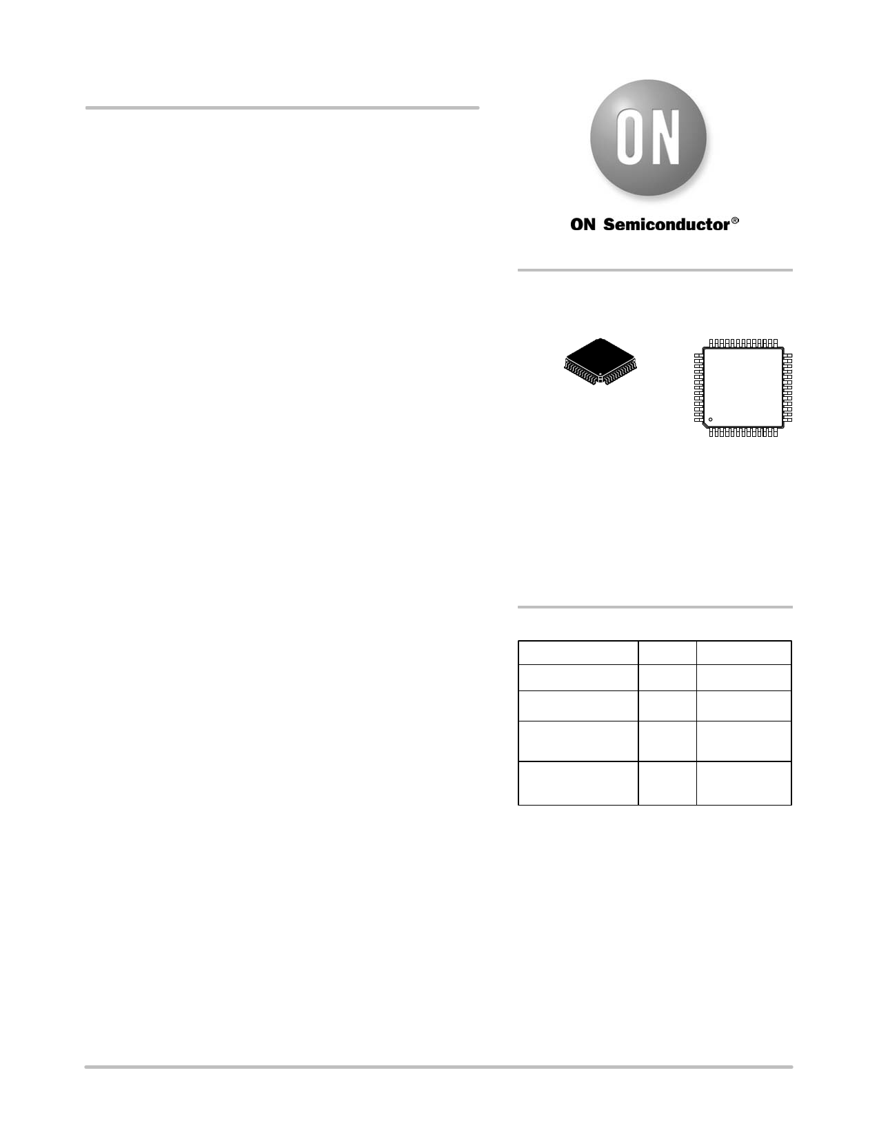
MARKING
DIAGRAM*
52−LEAD LQFP
THERMALLY ENHANCED
CASE 848H
FA SUFFIX
52
NB100
LVEP222
AWLYYWWG
1
A = Assembly Location
WL = Wafer Lot
YY = Year
WW = Work Week
G = Pb−Free Package
*For additional information, see Application Note
AND8002/D
ORDERING INFORMATION
Device
Package Shipping†
NB100LVEP222FA LQFP−52 160 Units/Tray
NB100LVEP222FAR2 LQFP−52 1500/Tape & Reel
NB100LVEP222FAG LQFP−52 160 Units/Tray
(Pb−Free)
NB100LVEP222FARG LQFP−52 1500/Tape & Reel
(Pb−Free)
†For information on tape and reel specifications,
including part orientation and tape sizes, please
refer to our Tape and Reel Packaging Specification
Brochure, BRD8011/D.
Publication Order Number:
NB100LVEP222/D
1 page 
NB100LVEP222
LVPECL DC CHARACTERISTICS VCC = VCC0 = 3.3 V; VEE = 0.0 V (Note 7)
−40°C
25°C
85°C
Symbol
IEE
VOH
VOL
VIH
VIL
VBB
VIHCMR
Characteristic
Power Supply Current
Output HIGH Voltage (Note 8)
Output LOW Voltage (Note 8)
Input HIGH Voltage (Single−Ended)
Input LOW Voltage (Single−Ended)
Output Reference Voltage (Note 9)
Input HIGH Voltage Common Mode
Range (Differential Configuration)
(Note 10) (Figure 5)
Min
100
2155
1355
2135
1355
1775
1.2
Typ
125
2280
1480
1875
Max
150
2405
1700
2420
1700
1975
3.3
Min
104
2155
1355
2135
1355
1775
1.2
Typ
130
2280
1480
1875
Max
156
2405
1700
2420
1700
1975
3.3
Min
112
2155
1355
2135
1355
1775
1.2
Typ
140
2280
1480
1875
Max
168
2405
1700
2420
1700
1975
3.3
Unit
mA
mV
mV
mV
mV
mV
V
IIH Input HIGH Current
150 150 150 mA
IIL Input LOW Current
CLK 0.5
CLK −150
0.5
−150
0.5
−150
mA
NOTE: 100LVEP circuits are designed to meet the DC specifications shown in the above table, after thermal equilibrium has been established.
The circuit is in a test socket or mounted on a printed circuit board and transverse air flow greater than 500 lfpm is maintained.
7. Input and output parameters vary 1:1 with VCC/VCC0. VEE can vary + 0.925 V to −0.5 V.
8. All loading with 50 W to VCC/VCC0−2.0 V.
9. Single ended input operation is limited VCC/VCC0 ≥ 3.0 V in LVPECL mode.
10. VIHCMR min varies 1:1 with VEE, VIHCMR max varies 1:1 with VCC/VCC0. The VIHCMR range is referenced to the most positive side of the
differential input signal.
LVNECL DC CHARACTERISTICS VCC = VCC0 = 0.0 V; VEE = −3.8 V to −2.375 V (Note 11)
−40°C
25°C
85°C
Symbol
Characteristic
Min Typ Max Min Typ Max Min Typ Max Unit
IEE
VOH
VOL
VIH
VIL
VBB
VIHCMR
Power Supply Current
Output HIGH Voltage (Note 12)
Output LOW Voltage (Note 12)
Input HIGH Voltage (Single Ended)
Input LOW Voltage (Single Ended)
Output Reference Voltage (Note 13)
Input HIGH Voltage Common Mode
Range (Differential Configuration)
(Note 14) (Figure 5)
100 125 150 104 130 156 112 140 168
−1145 −1020 −895 −1145 −1020 −895 −1145 −1020 −895
−1945 −1820 −1600 −1945 −1820 −1600 −1945 −1820 −1600
−1165
−880 −1165
−880 −1165
−880
−1945
−1600 −1945
−1600 −1945
−1600
−1525 −1425 −1325 −1525 −1425 −1325 −1525 −1425 −1325
VEE + 1.2 0.0 VEE + 1.2 0.0 VEE + 1.2 0.0
mA
mV
mV
mV
mV
mV
V
IIH Input HIGH Current
IIL Input LOW Current
CLK 0.5
CLK −150
150
0.5
−150
150
0.5
−150
150 mA
mA
NOTE: 100LVEP circuits are designed to meet the DC specifications shown in the above table, after thermal equilibrium has been established.
The circuit is in a test socket or mounted on a printed circuit board and transverse air flow greater than 500 lfpm is maintained.
11. Input and output parameters vary 1:1 with VCC/VCC0.
12. All loading with 50 W to VCC/VCC0 − 2.0 V.
13. Single ended input operation is limited VEE ≤ −3.0 V in NECL mode.
14. VIHCMR min varies 1:1 with VEE, VIHCMR max varies 1:1 with VCC/VCC0. The VIHCMR range is referenced to the most positive side of the
differential input signal.
http://onsemi.com
5
5 Page | ||
| Páginas | Total 10 Páginas | |
| PDF Descargar | [ Datasheet NB100LVEP222.PDF ] | |
Hoja de datos destacado
| Número de pieza | Descripción | Fabricantes |
| NB100LVEP221 | 1:20 Differential HSTL/ECL/PECL Clock Driver | ON Semiconductor |
| NB100LVEP222 | 1:15 Differential ECL/PECL /1 /2 Clock Driver | ON Semiconductor |
| NB100LVEP224 | 1:24 Differential ECL/PECL Clock Driver | ON Semiconductor |
| Número de pieza | Descripción | Fabricantes |
| SLA6805M | High Voltage 3 phase Motor Driver IC. |
Sanken |
| SDC1742 | 12- and 14-Bit Hybrid Synchro / Resolver-to-Digital Converters. |
Analog Devices |
|
DataSheet.es es una pagina web que funciona como un repositorio de manuales o hoja de datos de muchos de los productos más populares, |
| DataSheet.es | 2020 | Privacy Policy | Contacto | Buscar |