|
|
|
PDF ATA5757 Data sheet ( Hoja de datos )
| Número de pieza | ATA5757 | |
| Descripción | (ATA5756 / ATA5757) UHF ASK/FSK TRANSMITTER | |
| Fabricantes | ATMEL Corporation | |
| Logotipo | ||
Hay una vista previa y un enlace de descarga de ATA5757 (archivo pdf) en la parte inferior de esta página. Total 20 Páginas | ||
|
No Preview Available !
Features
• PLL Transmitter IC with Single-ended Output
• High Output Power (6 dBm) at 8.1 mA (315 MHz) and 8.5 mA (433 MHz) Typical Values
• Divide by 24 (ATA5756) and 32 (ATA5757) Blocks for 13 MHz Crystal Frequencies and
for Low XTO Start-up Times
• Modulation Scheme ASK/FSK with Internal FSK Switch
• Up to 20 kBaud Manchester Coding, Up to 40 kBaud NRZ Coding
• Power-down Idle and Power-up Modes to Adjust Corresponding Current Consumption
through ASK/FSK/Enable Input Pins
• ENABLE Input for Parallel Usage of Controlling Pins in a 3-wire Bus System
• CLK Output Switches ON if the Crystal Current Amplitude has Reached 35% to 80% of
its Final Value
• Crystal Oscillator Time Until CLK Output is Activated, Typically 0.6 ms
• Supply Voltage 2.0 V to 3.6 V in Operation Temperature Range of -40° C to 125° C
• ESD Protection at all Pins (4 kV HBM)
• Small Package MSOP10
Benefits
• Low Parasitic FSK Switch Integrated
• Very Short and Reproducible Time to Transmit Typically < 0.85 ms
• 13.125 MHz/13.56 MHz Crystals Give Opportunity for Small Package Sizes
UHF ASK/FSK
Transmitter
ATA5756
ATA5757
Description
The ATA5756/ATA5757 is a PLL transmitter IC which has been developed for the
demands of RF low-cost transmission systems at data rates up to 20 kBaud Manches-
ter coding and 40 kBaud NRZ coding. The transmitting frequency range is 313 MHz to
317 MHz (ATA5756) and 432 MHz to 448 MHz (ATA575w7w)w,.DraetaSshpeeet4Uc.ctoimvely. It can be used
in both FSK and ASK systems. Due to its shorten crystal oscillator settling time it is
well suited for Tire Pressure Monitoring (TPM) and for Passive Entry Go applications.
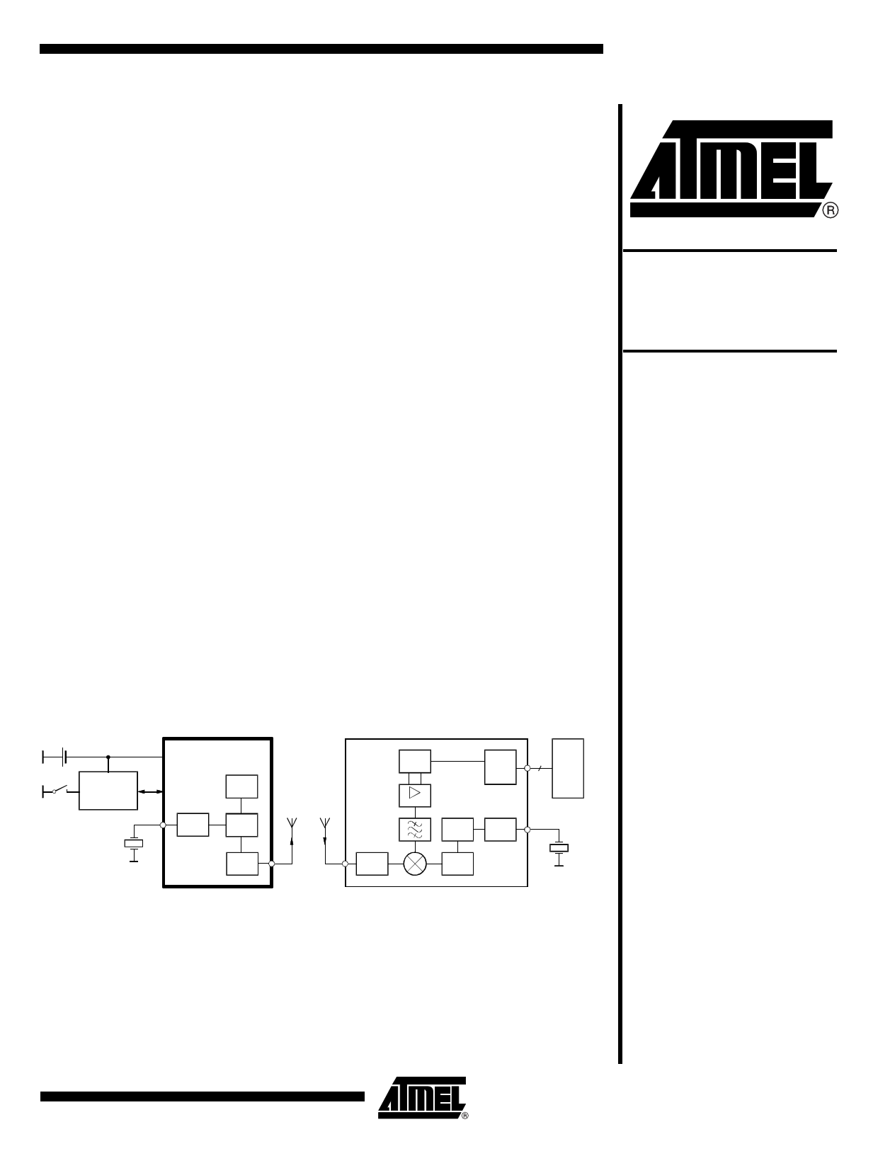
Figure 1. System Block Diagram
1 Li cell
Encoder
Keys ATARx9x
UHF ASK/FSK
TPM and Remote control
transmitter
ATA5756/
ATA5757
PLL
UHF ASK/FSK
Remote control receiver
U3741B/
U3745B/
T5743/
T5744/
Demod.
Control
XTO
VCO
Antenna Antenna
IF Amp
PLL
XTO
1...3
µC
Power
amp.
LNA
VCO
Rev. 4702H–RKE–09/04
1 page 
Functional
Description
4702H–RKE–09/04
ATA5756/ATA5757
The power amplifier is an open-collector output delivering a current pulse which is nearly
independent from the load impedance and can therefore be controlled via the connected
load impedance.
This output configuration enables a simple matching to any kind of antenna or to 50 Ω. A
high power efficiency for the power amplifier results if an optimized load impedance of
ZLoad, opt = 380 Ω + j340 Ω (ATA5756) at 315 MHz and ZLoad, opt = 280 Ω + j310 Ω
(ATA5757) at 433.92 MHz is used at the 3-V supply voltage.
If ASK = Low, FSK = Low and ENABLE = open or Low, the circuit is in power-down
mode consuming only a very small amount of current so that a lithium cell used as
power supply can work for many years.
If the ENABLE pin is left open, ENABLE is the logical OR operation of the ASK and FSK
input pins. This means, the IC can be switched on by either the FSK of the ASK input.
If the ENABLE pin is Low and ASK or FSK are High, the IC is in idle mode where the
PLL, XTO and power amplifier are off and the microcontroller ports controlling the ASK
and FSK inputs can be used to control other devices. This can help to save ports on the
microcontroller in systems where other devices with 3-wire interface are used.
With FSK = High and ASK = Low and ENABLE = open or High, the PLL and the XTO
are switched on and the power amplifier is off. When the amplitude of the current
through the crystal has reached 35% to 80% of its final amplitude, the CLK driver is
automatically activated. The CLK output stays Low until the CLK driver has been acti-
vated. The driver is activated synchronously with the CLK output frequency, hence, the
first pulse on the CLK output is a complete period. The PLL is then locked within
<250 µs after the CLK driver has been activated, and the transmitter is then ready for
data transmission.
With ASK = High the power amplifier is switched on. This is used to perform the ASK
modulation. During ASK modulation the IC is enabled with the FSK or the ENABLE pin.
With FSK = Low the switch at pin XTO2 is closed, with FSK = High the switch is open.
To achieve a faster start-up of the crystal oscillator, the FSK pin should be High during
start-up of the XTO because the series resistance of the resonator seen from pin XTO1
is lower if the switch is off.
The different modes of the ATA5756/ATA5757 are listed in Table 1, the corresponding
current consumption values can be found in the table “Electrical Characteristics” on
page 15.
Table 1. ATA5756/ATA5757 Modes
ASK Pin
FSK Pin
ENABLE Pin
Low Low Low/open
Low Low High
Low
High
High/open
High
Low
High/open
High
High
High/open
Low/High
High
Low
High
Low/High
Low
Mode
Power-down mode, FSK switch High Z
Power-up, PA off, FSK switch Low Z
Power-up, PA off, FSK switch High Z
Power-up, PA on, FSK switch Low Z
Power-up, PA on, FSK switch High Z
Idle mode, FSK switch High Z
Idle mode, FSK switch High Z
5
5 Page 
Application Circuits
ATA5756/ATA5757
For the supply voltage blocking capacitor C3, a value of 68 nF/X7R is recommended
(see Figure 10 on page 12 and Figure 11 on page 13). C1 and C2 are used to match the
loop antenna to the power amplifier. For C2, two capacitors in series should be used to
achieve a better tolerance value and to enable it to realize ZLoad,opt by using capacitors
with standard values.
Together with the pins of ATA5756 and the PCB board wires, C1 forms a series resonance
loop that suppresses the 1st harmonic, hence the position of C1 on the PCB is important.
Normally, the best suppression is achieved when C1 is placed as close as possible to
the pins ANT1 and ANT2.
The loop antenna should not exceed a width of 1.5 mm, otherwise the Q-factor of the
loop antenna is too high.
L1 (50 nH to 100 nH) can be printed on the PCB. C4 should be selected so that the XTO
runs on the load resonance frequency of the crystal. Normally, a value of 10 pF results
in a 12 pF load-capacitance crystal due to the board parasitic capacitances and the
inductive impedance of the XTO1 pin.
4702H–RKE–09/04
11
11 Page | ||
| Páginas | Total 20 Páginas | |
| PDF Descargar | [ Datasheet ATA5757.PDF ] | |
Hoja de datos destacado
| Número de pieza | Descripción | Fabricantes |
| ATA5756 | (ATA5756 / ATA5757) UHF ASK/FSK TRANSMITTER | ATMEL Corporation |
| ATA5757 | (ATA5756 / ATA5757) UHF ASK/FSK TRANSMITTER | ATMEL Corporation |
| Número de pieza | Descripción | Fabricantes |
| SLA6805M | High Voltage 3 phase Motor Driver IC. |
Sanken |
| SDC1742 | 12- and 14-Bit Hybrid Synchro / Resolver-to-Digital Converters. |
Analog Devices |
|
DataSheet.es es una pagina web que funciona como un repositorio de manuales o hoja de datos de muchos de los productos más populares, |
| DataSheet.es | 2020 | Privacy Policy | Contacto | Buscar |