|
|
|
PDF ISL22449 Data sheet ( Hoja de datos )
| Número de pieza | ISL22449 | |
| Descripción | Quad Digitally Controlled Potentiometer | |
| Fabricantes | Intersil Corporation | |
| Logotipo | ||
Hay una vista previa y un enlace de descarga de ISL22449 (archivo pdf) en la parte inferior de esta página. Total 12 Páginas | ||
|
No Preview Available !
ISL22449
® Quad Digitally Controlled Potentiometer (XDCP™)
Data Sheet
September 15, 2006
FN6333.2
Low Noise, Low Power, SPI® Bus, 128 Taps,
Wiper Only
The ISL22449 integrates four digitally controlled
potentiometers (DCP) and non-volatile memory on a
monolithic CMOS integrated circuit.
The digitally controlled potentiometers are implemented with
a combination of resistor elements and CMOS switches. The
position of the wipers are controlled by the user through the
SPI serial interface. Each potentiometer has an associated
volatile Wiper Register (WR) and a non-volatile Initial Value
Register (IVR) that can be directly written to and read by the
user. The contents of the WR controls the position of the
wiper. At power-up the device recalls the contents of the
DCP’s IVR to the corresponding WR.
The DCP can be used as a voltage divider in a wide variety
of applications including control, parameter adjustments, AC
measurement and signal processing.
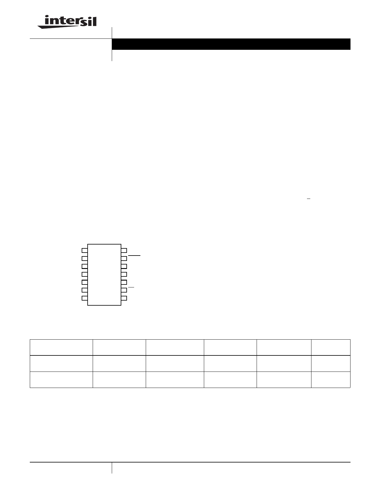
Pinout
www.DataSheet4U.com
ISL22449
(14 LD TSSOP)
TOP VIEW
RW3
NC
SCK
SDO
GND
RW2
RW1
1
2
3
4
5
6
7
14 RW0
13 SHDN
12 VCC
11 NC
10 SDI
9 CS
8 NC
Features
• Four potentiometers in one package
• 128 resistor taps
• SPI serial interface
• Non-volatile storage of wiper position
• Wiper resistance: 70Ω typical
• Shutdown mode
• Shutdown current 6.5µA max
• Power supply: 2.7V to 5.5V
• 50kΩ or 10kΩ total resistance
• High reliability
- Endurance: 1,000,000 data changes per bit per register
- Register data retention: 50 years @ T < +55°C
• 14 Lead TSSOP
• Pb-free plus anneal product (RoHS compliant)
Ordering Information
PART NUMBER
PART MARKING
RESISTANCE OPTION
(kΩ)
TEMP. RANGE
(°C)
PACKAGE
PKG. DWG. #
ISL22449UFV14Z
(Notes 1, 2)
22449 UFVZ
50
-40 to +125
14 Ld TSSOP
M14.173
(Pb-free)
ISL22449WFV14Z
(Notes 1, 2)
22449 WFVZ
10
-40 to +125
14 Ld TSSOP
M14.173
(Pb-free)
NOTES:
1. Intersil Pb-free plus anneal products employ special Pb-free material sets; molding compounds/die attach materials and 100% matte tin plate
termination finish, which are RoHS compliant and compatible with both SnPb and Pb-free soldering operations. Intersil Pb-free products are
MSL classified at Pb-free peak reflow temperatures that meet or exceed the Pb-free requirements of IPC/JEDEC J STD-020.
2. Add “-TK” suffix for 1,000 Tape and Reel option
1 CAUTION: These devices are sensitive to electrostatic discharge; follow proper IC Handling Procedures.
1-888-INTERSIL or 1-888-468-3774 | Intersil (and design) and XDCP are registered trademarks of Intersil Americas Inc.
Copyright Intersil Americas Inc. 2006. All Rights Reserved
All other trademarks mentioned are the property of their respective owners.
1 page 
ISL22449
Operating Specifications Over the recommended operating conditions unless otherwise specified. (Continued)
SYMBOL
PARAMETER
TEST CONDITIONS
TYP
MIN (NOTE 5) MAX
UNIT
Hysteresis SHDN, SCK, SDI, and CS input buffer
hysteresis
VOL
Rpu
(Note 14)
SDO output buffer LOW voltage
SDO pull-up resistor off-chip
IOL = 4mA
Maximum is determined by tRO and tFO with
maximum bus load Cbus = 30pF, fSCK =
5MHz
0.05*
VCC
0
V
0.4 V
2 kΩ
Cpin SHDN, SCK, SDI, SDO and CS pin
(Note 15) capacitance
10 pF
fSCK
tCYC
tWH
tWL
tLEAD
tLAG
tSU
tH
tRI
tFI
tDIS
tV
tHO
tRO
tFO
tCS
tWRT
SPI frequency
SPI clock cycle time
SPI clock high time
SPI clock low time
Lead time
Lag time
SDI, SCK and CS input setup time
SDI, SCK and CS input hold time
SDI, SCK and CS input rise time
SDI, SCK and CS input fall time
SDO output Disable time
SDO output valid time
SDO output hold time
SDO output rise time
SDO output fall time
CS deselect time
Rpu = 2k, Cbus = 30pF
Rpu = 2k, Cbus = 30pF
Wiper Response Time after SPI write
to WR register
5 MHz
200 ns
100 ns
100 ns
250 ns
250 ns
50 ns
50 ns
10 ns
10 20 ns
0 100 ns
350 ns
0 ns
60 ns
60 ns
2 µs
1.5 µs
NOTES:
5. Typical values are for TA = +25°C and 3.3V supply voltage.
6. LSB: [V(RW)127 – V(RW)0]/127. V(RW)127 and V(RW)0 are V(RW) for the DCP register set to 7F hex and 00 hex respectively. LSB is the
incremental voltage when changing from one tap to an adjacent tap.
7. ZS error = V(RW)0/LSB.
8. FS error = [V(RW)127 – VCC]/LSB.
9. DNL = [V(RW)i – V(RW)i-1]/LSB-1, for i = 1 to 127. i is the DCP register setting.
10. INL = [V(RW)i – i • LSB – V(RW)]/LSB for i = 1 to 127
11. VMATCH = [V(RWx)i – V(RWy)i]/LSB, for i = 1 to 127, x = 0 to 3 and y = 0 to 3.
12.
TCV
=
-------M-----a----x----(--V----(---R-----W------)--i--)---–-----M-----i--n----(--V-----(--R-----W------)--i--)------ × ----1---0----6----- for i = 16 to 112 decimal, T = -40°C to +125°C. Max( ) is the maximum value of the wiper
[Max(V(RW)i) + Min(V(RW)i)] ⁄ 2 165°C voltage and Min ( ) is the minimum value of the wiper voltage over the temperature range.
13. tWC is the time from the end of a Write sequence of SPI serial interface, to the end of the self-timed internal non-volatile write cycle.
14. Rpu is specified for the highest data rate transfer for the device. Higher value pullup can be used at lower data rates.
15. This parameter is not 100% tested.
5 FN6333.2
September 15, 2006
5 Page 
ISL22449
CS
SCK
SDI DON’T CARE
0 1 0 1 0 0 0 0 0 I3 I2 I1 I0 R3 R2 R1 R0
SDO
0
FIGURE 13. THREE BYTE READ SEQUENCE
D6 D5 D4 D3 D2 D1 D0
Applications Information
Communicating with ISL22449
Communication with ISL22449 proceeds using SPI interface
through the ACR (address 1000b), IVRi (addresses 0000b,
0001b, 0010b and 0011b) and WRi (addresses 0000b,
0001b, 0010b and 0011b) registers.
The wiper of the potentiometer is controlled by the WRi
register. Writes and reads can be made directly to these
registers to control and monitor the wiper position without
any non-volatile memory changes. This is done by setting
MSB bit at address 1000b to 1.
The non-volatile IVRi stores the power up value of the wiper.
IVRs are accessible when MSB bit at address 1000b is set
to 0. Writing a new value to the IVRi register will set a new
power up position for the wiper. Also, writing to this register
will load the same value into the corresponding WRi as the
IVRi. Reading from the IVRi will not change the WRi, if its
contents are different.
Examples:
A. Writing to the IVR:
This sequence will write a new value (77h) to the IVR2(non-volatile):
Set the ACR (Addr 1000b) for NV write (40h)
Send the ID byte, Instruction Byte, then the Data byte
010100001100100001000000
(Sent to SDI)
Set the IVR (Addr 0010b) to 77h
Send the ID byte, Instruction Byte, then the Data byte
010100001100001001110111
(Sent to SDI)
B. Reading from the WR:
This sequence will read the value from the WR3 (volatile):
Write to ACR first to access the volatile WRs
Send the ID byte, Instruction Byte, then the Data byte
010100001100100011000000
(Sent to SDI)
Read the data from WR3 (Addr 0011b)
Send the ID byte, Instruction Byte, then Read the Data byte
0101000010110011xxxxxxxx
(Out on SDO)
11 FN6333.2
September 15, 2006
11 Page | ||
| Páginas | Total 12 Páginas | |
| PDF Descargar | [ Datasheet ISL22449.PDF ] | |
Hoja de datos destacado
| Número de pieza | Descripción | Fabricantes |
| ISL22444 | Quad Digitally Controlled Potentiometer | Intersil |
| ISL22446 | Quad Digitally Controlled Potentiometer | Intersil Corporation |
| ISL22449 | Quad Digitally Controlled Potentiometer | Intersil Corporation |
| Número de pieza | Descripción | Fabricantes |
| SLA6805M | High Voltage 3 phase Motor Driver IC. |
Sanken |
| SDC1742 | 12- and 14-Bit Hybrid Synchro / Resolver-to-Digital Converters. |
Analog Devices |
|
DataSheet.es es una pagina web que funciona como un repositorio de manuales o hoja de datos de muchos de los productos más populares, |
| DataSheet.es | 2020 | Privacy Policy | Contacto | Buscar |