|
|
|
PDF X9260 Data sheet ( Hoja de datos )
| Número de pieza | X9260 | |
| Descripción | Dual Digitally-Controlled Potentiometers | |
| Fabricantes | Intersil Corporation | |
| Logotipo | ||
Hay una vista previa y un enlace de descarga de X9260 (archivo pdf) en la parte inferior de esta página. Total 23 Páginas | ||
|
No Preview Available !
®
Data Sheet
X9260
Dual Supply/Low Power/256-Tap/SPI bus
August 29, 2006
FN8170.3
Dual Digitally-Controlled (XDCP™)
Potentiometers
FEATURES
• Dual–Two Separate Potentiometers
• 256 Resistor Taps/pot–0.4% Resolution
• SPI Serial Interface for Write, Read, and Transfer
Operations of the Potentiometer
• Wiper Resistance, 100Ω typical @ V+ = 5V,
V- = -5V
• 4 Nonvolatile Data Registers for Each
Potentiometer
• Nonvolatile Storage of Multiple Wiper Positions
• Power-on Recall. Loads Saved Wiper Position
on Power-up.
• Standby Current <5µA Max
• VCC: 2.7V to 5.5V Operation
• 50kΩ, 100kΩ Versions of End to End Resistance
• 100 yr. Data Retention
• Endurance: 100,000 Data Changes per Bit per
Register
• 24 Ld SOIC
• Low Power CMOS
•www.DataSheet4U.com Power Supply VCC = 2.7V to 5.5V
V+ = 2.7V to 5.5V
V- = -2.7V to -5.5V
• Pb-Free Plus Anneal Available (RoHS Compliant)
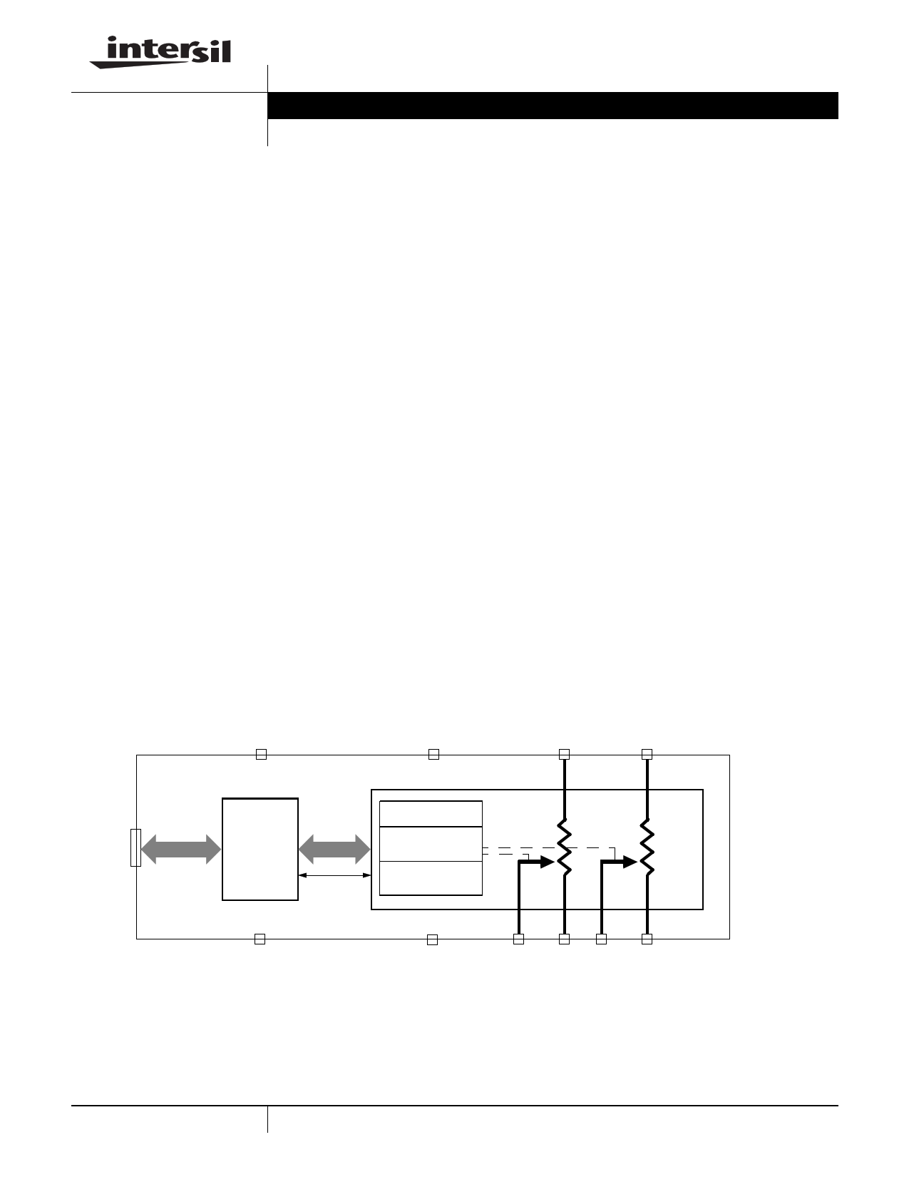
FUNCTIONAL DIAGRAM
DESCRIPTION
The X9260 integrates 2 digitally controlled
potentiometer (XDCP) on a monolithic CMOS
integrated circuit.
The digitally controlled potentiometer is implemented
using 255 resistive elements in a series array.
Between each element are tap points connected to the
wiper terminal through switches. The position of the
wiper on the array is controlled by the user through the
SPI bus interface. Each potentiometer has associated
with it a volatile Wiper Counter Register (WCR) and a
four nononvolatile Data Registers that can be directly
written to and read by the user. The contents of the
WCR controls the position of the wiper on the resistor
array though the switches. Power-up recalls the
contents of the default Data Register (DR0) to the
WCR.
The XDCP can be used as a three-terminal
potentiometer or as a two terminal variable resistor in
a wide variety of applications including control,
parameter adjustments, and signal processing.
VCC
V+
RH0
RH1
SPI
Bus
Interface
Address
Data
Status
Bus
Interface
and Control
Write
Read
Transfer
Inc/Dec
Control
Power-on Recall
Wiper Counter
Registers (WCR)
Data Registers
(DR0-DR3)
VSS
V- RW0 RL0 RW1 RL1
50kΩ or 100kΩ versions
1 CAUTION: These devices are sensitive to electrostatic discharge; follow proper IC Handling Procedures.
1-888-INTERSIL or 1-888-468-3774 | Intersil (and design) is a registered trademark of Intersil Americas Inc.
XDCP is a trademark of Intersil Americas Inc. Copyright Intersil Americas Inc. 2005, 2006. All Rights Reserved
All other trademarks mentioned are the property of their respective owners
1 page 
X9260
standby state. CS LOW enables the X9260, placing it
in the active power mode. It should be noted that after
a power-up, a HIGH to LOW transition on CS is
required prior to the start of any operation.
Potentiometer Pins
RH, RL
The RH and RL pins are equivalent to the terminal
connections on a mechanical potentiometer. Since
there are 2 potentiometers, there are 2 sets of RH and
RL such that RH0 and RL0 are the terminals of POT 0
and so on.
RW
The wiper pin are equivalent to the wiper terminal of a
mechanical potentiometer. Since there are 2
potentiometers, there are 2 sets of RW such that RW0
is the terminals of POT 0 and so on.
Supply Pins
SYSTEM SUPPLY VOLTAGE (VCC) AND SUPPLY
GROUND (VSS)
The VCC pin is the system supply voltage. The VSS
pin is the system ground.
Analog Supply Voltages (V+ and V-)
These supplies are the analog voltage supplies for the
potentiometer. The V+ supply is tied to the wiper
switches while the V- supply is used to bias the
switches and the internal P+ substrate of the
integrated circuit. Both of these supplies set the
voltage limits of the potentiometer.
Other Pins
NO CONNECT
No connect pins should be left floating. This pins are
used for Intersil manufacturing and testing purposes.
HARDWARE WRITE PROTECT INPUT (WP)
The WP pin when LOW prevents nonvolatile writes to
the Data Registers.
PRINCIPLES OF OPERATION
Serial Interface
The X9260 supports the SPI interface hardware
conventions. The device is accessed via the SI input
with data clocked in on the rising SCK. CS must be
LOW and the HOLD and WP pins must be HIGH
during the entire operation.
The SO and SI pins can be connected together, since
they have three state outputs. This can help to reduce
system pin count.
Array Description
The X9260 is comprised of a resistor array (See
Figure 1). The array contains the equivalent of 255
discrete resistive segments that are connected in
series. The physical ends of each array are equivalent
to the fixed terminals of a mechanical potentiometer
(RH and RL inputs).
At both ends of each array and between each resistor
segment is a CMOS switch connected to the wiper
(RW) output. Within each individual array only one
switch may be turned on at a time.
These switches are controlled by a Wiper Counter
Register (WCR). The 8-bits of the WCR (WCR[7:0])
are decoded to select, and enable, one of 256
switches (See Table 1).
Power-up and Down Requirements.
At all times, the voltages on the potentiometer pins
must be less than V+ and more than V-. During power-
up and power-down, VCC, V+, and V- must reach their
final values within 1msecs of each other. The VCC
ramp rate spec is always in effect.
5 FN8170.3
August 29, 2006
5 Page 
X9260
Table 5. Instruction Set
Instruction Set
Instruction
I3 I2 I1 I0 RB RA 0 P0
Operation
Read Wiper Counter
Register
10010 0
0 1/0 Read the contents of the Wiper Counter
Register pointed to by P0
Write Wiper Counter
Register
10100 0
0 1/0 Write new value to the Wiper Counter
Register pointed to by P0
Read Data Register
1 0 1 1 1/0 1/0 0 1/0 Read the contents of the Data Register
pointed to by P0 and RB - RA
Write Data Register
1 1 0 0 1/0 1/0 0 1/0 Write new value to the Data Register
pointed to by P0 and RB - RA
XFR Data Register to
Wiper Counter Register
1 1 0 1 1/0 1/0 0 1/0 Transfer the contents of the Data Register
pointed to by P0 and RB - RA to its
associated Wiper Counter Register
XFR Wiper Counter
Register to Data Register
1 1 1 0 1/0 1/0 0 1/0 Transfer the contents of the Wiper Counter
Register pointed to by P0 to the Data
Register pointed to by RB - RA
Global XFR Data Registers 0 0 0 1 1/0 1/0 0
to Wiper Counter Registers
0 Transfer the contents of the Data Registers
pointed to by RB - RA of all four pots to their
respective Wiper Counter Registers
Global XFR Wiper Counter 1 0 0 0 1/0 1/0 0
Registers to Data Register
0 Transfer the contents of both Wiper Counter
Registers to their respective data Registers
pointed to by RB - RA of all four pots
Increment/Decrement
Wiper Counter Register
00100 0
0 1/0 Enable Increment/decrement of the Control
Latch pointed to by P0
Note: 1/0 = data is one or zero
11 FN8170.3
August 29, 2006
11 Page | ||
| Páginas | Total 23 Páginas | |
| PDF Descargar | [ Datasheet X9260.PDF ] | |
Hoja de datos destacado
| Número de pieza | Descripción | Fabricantes |
| X9260 | Dual Digitally-Controlled Potentiometers | Intersil Corporation |
| X9261 | Dual Digitally-Controlled Potentiometers | Intersil Corporation |
| X9268 | Dual Digitally-Controlled Potentiometers | Intersil Corporation |
| X9269 | Dual Digitally-Controlled Potentiometers | Xicor |
| Número de pieza | Descripción | Fabricantes |
| SLA6805M | High Voltage 3 phase Motor Driver IC. |
Sanken |
| SDC1742 | 12- and 14-Bit Hybrid Synchro / Resolver-to-Digital Converters. |
Analog Devices |
|
DataSheet.es es una pagina web que funciona como un repositorio de manuales o hoja de datos de muchos de los productos más populares, |
| DataSheet.es | 2020 | Privacy Policy | Contacto | Buscar |