|
|
|
PDF X9410 Data sheet ( Hoja de datos )
| Número de pieza | X9410 | |
| Descripción | Dual Digitally Controlled Potentiometer | |
| Fabricantes | Intersil Corporation | |
| Logotipo | ||
Hay una vista previa y un enlace de descarga de X9410 (archivo pdf) en la parte inferior de esta página. Total 21 Páginas | ||
|
No Preview Available !
®
Data Sheet
X9410
Low Noise/Low Power/SPI Bus
October 12, 2006
FN8193.2
Dual Digitally Controlled Potentiometer
(XDCP™)
FEATURES
• Two potentiometers per package
• SPI serial interface
• Register oriented format
- Direct read/write/transfer wiper positions
- Store as many as four positions per
potentiometer
• Power supplies
- VCC = 2.7V to 5.5V
- V+ = 2.7V to 5.5V
- V- = -2.7V to -5.5V
• Low power CMOS
- Standby current < 1µA
- High reliability
- Endurance - 100,000 data changes per bit per
register
- Register data retention - 100 years
• 8-bytes of nonvolatile EEPROM memory
•www.DataSheet4U.com 10kΩ resistor arrays
• Resolution: 64 taps each pot
• 24 Ld SOIC, 24 Ld TSSOP, and 24 Ld plastic DIP
packages
• Pb-free plus anneal available (RoHS compliant)
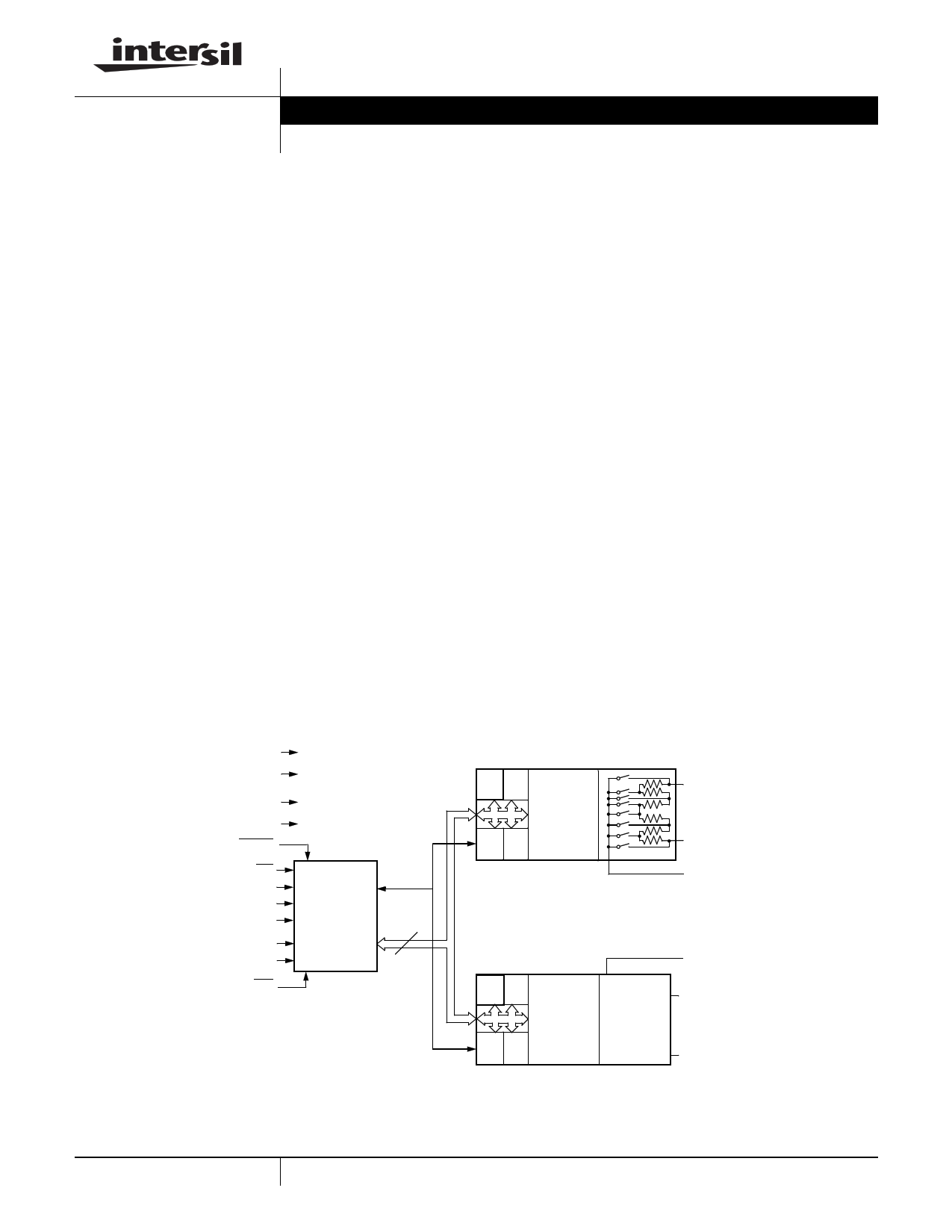
BLOCK DIAGRAM
VCC
VSS
V+
V-
HOLD
CS
SCK
SO
SI
A0
A1
WP
Interface
and
Control
Circuitry
8
Data
DESCRIPTION
The X9410 integrates two digitally controlled
potentiometers (XDCPs) on a monolithic CMOS
integrated circuit.
The digitally controlled potentiometer is implemented
using 63 resistive elements in a series array. Between
each element are tap points connected to the wiper
terminal through switches. The position of the wiper on
the array is controlled by the user through the SPI
serial bus interface. Each potentiometer has
associated with it a volatile Wiper Counter Register
(WCR) and four nonvolatile Data Registers (DR0:DR3)
that can be directly written to and read by the user.
The contents of the WCR controls the position of the
wiper on the resistor array through the switches.
Power-up recalls the contents of DR0 to the WCR.
The XDCP can be used as a three-terminal
potentiometer or as a two-terminal variable resistor in
a wide variety of applications including control,
parameter adjustments, and signal processing.
Pot 0
R0 R1
R2 R3
Wiper
Counter
Register
(WCR)
VH0/RH0
VL0/RL0
VW0/RW0
Pot 1
R0 R1
R2 R3
Wiper
Counter
Register
(WCR)
Resistor
Array
Pot1
VW1/RW1
VH1/RH1
VL1/RL1
1 CAUTION: These devices are sensitive to electrostatic discharge; follow proper IC Handling Procedures.
1-888-INTERSIL or 1-888-468-3774 | Intersil (and design) is a registered trademark of Intersil Americas Inc.
XDCP is a trademark of Intersil Americas Inc. Copyright Intersil Americas Inc. 2005-2006. All Rights Reserved
All other trademarks mentioned are the property of their respective owners.
1 page 
X9410
Write in Process
The contents of the Data Registers are saved to
nonvolatile memory when the CS pin goes from LOW
to HIGH after a complete write sequence is received
by the device. The progress of this internal write
operation can be monitored by a Write In Process bit
(WIP). The WIP bit is read with a Read Status
command.
INSTRUCTIONS
Identification (ID) Byte
The first byte sent to the X9410 from the host,
following a CS going HIGH to LOW, is called the
Identification byte. The most significant four bits of the
slave address are a device type identifier, for the
X9410 this is fixed as 0101[B] (refer to Figure 2).
The two least significant bits in the ID byte select one
of four devices on the bus. The physical device
address is defined by the state of the A0 - A1 input
pins. The X9410 compares the serial data stream with
the address input state; a successful compare of both
address bits is required for the X9410 to successfully
continue the command sequence. The A0 - A1 inputs
can be actively driven by CMOS input signals or tied to
VCC or VSS.
The remaining two bits in the ID byte must be set to 0.
Figure 2. Identification Byte Format
Device Type
Identifier
0 1 0 1 0 0 A1 A0
Device Address
Instruction Byte
The next byte sent to the X9410 contains the
instruction and register pointer information. The four
most significant bits are the instruction. The next four
bits point to one of the two pots and when applicable
they point to one of four associated registers. The
format is shown below in Figure 3.
Figure 3. Instruction Byte Format
Register
Select
I3 I2 I1 I0 R1 R0 0 P0
Instructions
Pot Select
The four high order bits of the instruction byte specify
the operation. The next two bits (R1 and R0) select one
of the four registers that is to be acted upon when a
register oriented instruction is issued. The last bit (P0)
selects which one of the two potentiometers is to be
affected by the instruction.
Four of the ten instructions are two bytes in length and
end with the transmission of the instruction byte.
These instructions are:
– XFR Data Register to Wiper Counter Register—This
transfers the contents of one specified Data Register
to the associated Wiper Counter Register.
– XFR Wiper Counter Register to Data Register—This
transfers the contents of the specified Wiper
Counter Register to the specified associated Data
Register.
– Global XFR Data Register to Counter Register—This
transfers the contents of both specified Data Registers
to the associated Wiper Counter Registers.
– Global XFR Wiper Counter Register to Data
Register—This transfers the contents of both Wiper
Counter Registers to the specified associated Data
Registers.
The basic sequence of the two byte instructions is
illustrated in Figure 4. These two-byte instructions
exchange data between the WCR and one of the data
registers. A transfer from a Data Register to a WCR is
essentially a write to a static RAM, with the static RAM
controlling the wiper position. The response of the
wiper to this action will be delayed by tWRL. A transfer
from the WCR (current wiper position), to a data
register is a write to nonvolatile memory and takes a
minimum of tWR to complete. The transfer can occur
between one of the two potentiometers and one of its
associated registers; or it may occur globally, where
the transfer occurs between both potentiometers and
one associated register.
5 FN8193.2
October 12, 2006
5 Page 
X9410
D.C. OPERATING CHARACTERISTICS (Over the recommended operating conditions unless otherwise specified.)
Symbol
ICC1
ICC2
ISB
ILI
ILO
VIH
VIL
VOL
Parameter
VCC supply current (Active)
VCC supply current (Nonvolatile
Write)
VCC current (standby)
Input leakage current
Output leakage current
Input HIGH voltage
Input LOW voltage
Output LOW voltage
Min.
VCC x 0.7
-0.5
Limits
Typ. Max.
400
1
1
10
10
VCC + 0.5
VCC x 0.1
0.4
Units
µA
mA
µA
µA
µA
V
V
V
Test Conditions
fSCK = 2MHz, SO = Open,
Other Inputs = VSS
fSCK = 2MHz, SO = Open,
Other Inputs = VSS
SCK = SI = VSS, Addr. = VSS
VIN = VSS to VCC
VOUT = VSS to VCC
IOL = 3mA
ENDURANCE AND DATA RETENTION
Parameter
Minimum endurance
Data retention
Min.
100,000
100
Unit
Data changes per bit per register
years
CAPACITANCE
Symbol
COUT(5)
CIN(5)
Test
Output capacitance (SO)
Input capacitance (A0, A1, SI, and SCK)
POWER-UP TIMING
Symbol
tPUR(6)
tPUW(6)
tR VCC
Parameter
Power-up to initiation of read operation
Power-up to initiation of write operation
VCC Power-up ramp
POWER-UP AND POWER-DOWN
There are no restrictions on the power-up or power-
down sequencing of the bias supplies VCC, V+, and V-
provided that all three supplies reach their final values
within 1msec of each other. However, at all times, the
voltages on the potentiometer pins must be less than
V+ and more than V-. The recall of the wiper position
from nonvolatile memory is not in effect until all
supplies reach their final value.
Max.
8
6
Unit
pF
pF
Test Conditions
VOUT = 0V
VIN = 0V
Min.
1
5
0.2
Max.
1
5
50
Unit
ms
ms
V/msec
EQUIVALENT A.C. LOAD CIRCUIT
SDA Output
5V
1533Ω
100pF
2.7V
100pF
11 FN8193.2
October 12, 2006
11 Page | ||
| Páginas | Total 21 Páginas | |
| PDF Descargar | [ Datasheet X9410.PDF ] | |
Hoja de datos destacado
| Número de pieza | Descripción | Fabricantes |
| X9410 | Dual Digitally Controlled Potentiometer | Xicor |
| X9410 | Dual Digitally Controlled Potentiometer | Intersil Corporation |
| X9418 | Dual Digitally Controlled Potentiometers | Xicor |
| X9418 | Dual Digitally Controlled Potentiometers | Intersil Corporation |
| Número de pieza | Descripción | Fabricantes |
| SLA6805M | High Voltage 3 phase Motor Driver IC. |
Sanken |
| SDC1742 | 12- and 14-Bit Hybrid Synchro / Resolver-to-Digital Converters. |
Analog Devices |
|
DataSheet.es es una pagina web que funciona como un repositorio de manuales o hoja de datos de muchos de los productos más populares, |
| DataSheet.es | 2020 | Privacy Policy | Contacto | Buscar |