|
|
PDF IS23SC4442 Data sheet ( Hoja de datos )
| Número de pieza | IS23SC4442 | |
| Descripción | 256 BYTE EEPROM | |
| Fabricantes | ISSI | |
| Logotipo |  |
|
Hay una vista previa y un enlace de descarga de IS23SC4442 (archivo pdf) en la parte inferior de esta página. Total 21 Páginas | ||
|
No Preview Available !
IS23SC4442
ISSI®
256 BYTE EEPROM
WITH WRITE PROTECT FUNCTION AND
PROGRAMMABLE SECURITY
PRELIMINARY INFORMATION
August 2003
FEATURES
• Standard CMOS process
• 256 x 8 bits EEPROM organization
• Byte-wise addressing
• Irreversible byte-wise write protection of lowest
32 address (Byte 0..31)
• 3-byte Programmable Security Code (PSC) for
memory write/erase protection
• 2.7-5.5V power supply for read and write/erase
• Low power operation: 3 mA typical active current
• 2.5 ms programming time
• 2-wire serial interface
www.DataSheet4U.com
• End of processing indication
• ISO standard 7816 compatible
• High reliability:
– 1,000,000 erase/write cycles guaranteed
– 10 years data retention
• Wide operating temperature range
–30oC to 75oC
DESCRIPTION
IS23SC4442 contains 256 x 8 bits of EEPROM main
memory and a 32 x 1 bit protection PROM memory.
The main memory can be randomly accessed byte by
byte. During memory erase, all 8 bits of a byte are set
to logical one. During memory write, individual bit(s)
are set to logical zeros depend on the data value to be
written. Normally, a data change may consists of an
erase and a write operation. The write or erase operation
takes at least 2.5 ms to complete.
The first 32 bytes (Address: 0 to 31) in memory are
irreversibly protected by the corresponding 32 protect
bits in the 32 x 1 bit protection memory. The 32 protect
bits are onetime programmable, and they cannot be
erased once they are set to logical zero.
IS23SC4442 provides a 3-bit Error Counter (EC), and
three bytes Programmable Security Code (PSC) to
prevent unauthorized erase/write operation to the
memory. All the memory, except the PSC, can be read
after the chip is powered on. But, the memory can be
written or erased only after the PSC is entered and
verified correct. After three successive unsuccessful
verifications of PSC, the Error Counter locks the chip
from a further attempt, and the memory can never be
erased or written.
Copyright © 2003 Integrated Silicon Solution, Inc. All rights reserved. ISSI reserves the right to make changes to this specification and its products at any time without notice. ISSI assumes no liability
arising out of the application or use of any information, products or services described herein. Customers are advised to obtain the latest version of this device specification before relying on any
published information and before placing orders for products.
Integrated Silicon Solution, Inc. — www.issi.com — 1-800-379-4774
Rev. 00B
08/01/03
1
1 page 
IS23SC4442
ISSI®
Functional Description
The IS23SC4442 contains 256 bytes of EEPROM main
memory (see block diagram) and a 32 bit protection
memory. The main memory is byte-wise erased and
written. When the memory is erased, 8 bits of the data
byte are all set to logic 1. When the memory is written, a
data byte can be programmed bit by bit, and it is set to
logic 0 according to the logic between the old and new
data. Generally, updating data includes an erase and
write procedure. When updated, new input data and the
contents of the old data are compared. If none of the 8
bits requires a logic 0 to 1 change, the erase operation
will be skipped. On the contrary, the write operation will
be skipped if no logic 1 to 0 change is necessary. The
write and erase operation takes at least 2.5 ms each.
The first 32 bytes can be protected individually by writing
the corresponding bit in the protection memory. Each
data byte in the address range and its assigned bit in the
protection memory have the same address. Once the
protection bit is written it cannot be erased.
The security memory of IS23SC4442 contains an error
counter (bit 0-bit 2) and 3 bytes reference data. The three
bytes reference data are as a whole called programmable
security code (PSC). After power on, except for the
PSC, the whole memory can always be read. The error
counter can always be written. After three successive
unsuccessful PSC verifications, the error counter will
block the chip, and write and erase operation to the
memory will be forbidden.
TRANSMISSION PROTOCOL
Transmission Mode
The transmission protocol is a two-wire link protocol
between the interface device IFD and IC. The protocol
type is "S = 10". All data changes on I/O are triggered by
the falling edge on CLK.
The transmission protocol is composed of the following
four modes:
– Reset and answer- to-reset
– Command mode
– Data output mode
– Processing mode
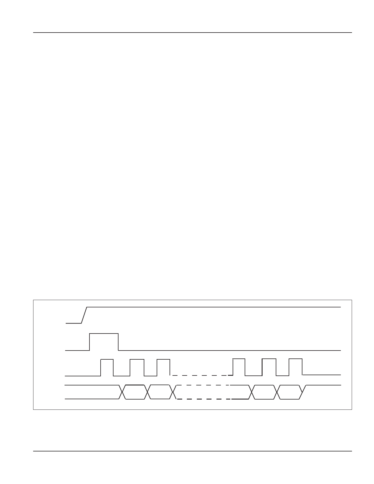
Reset and Answer-To-Reset
According to IS07816-3, Answer-To-Reset takes place
during operation. The reset can be implemented at any
time. During reset, the address counter is set to zero.
When RST is set from high level to low level, the lowest
bit of the first byte is read on the I/O. Under continuous
31 clock pulses, the contents of the first 4 byte EEPROM
addresses can be read out. The 33rd clock pulse sets
the I/O to high impedance. During Answer-To-Reset, any
start and stop condition is ignored.
Vcc
RST
CLK
I/O
1 23
31 32
IC sets I/O high
impedance
1 23
Figure: Reset and Answer-To-Reset
31 32
Integrated Silicon Solution, Inc. — www.issi.com — 1-800-379-4774
Rev. 00B
08/01/03
5
5 Page 
IS23SC4442
ISSI®
Read Security Memory
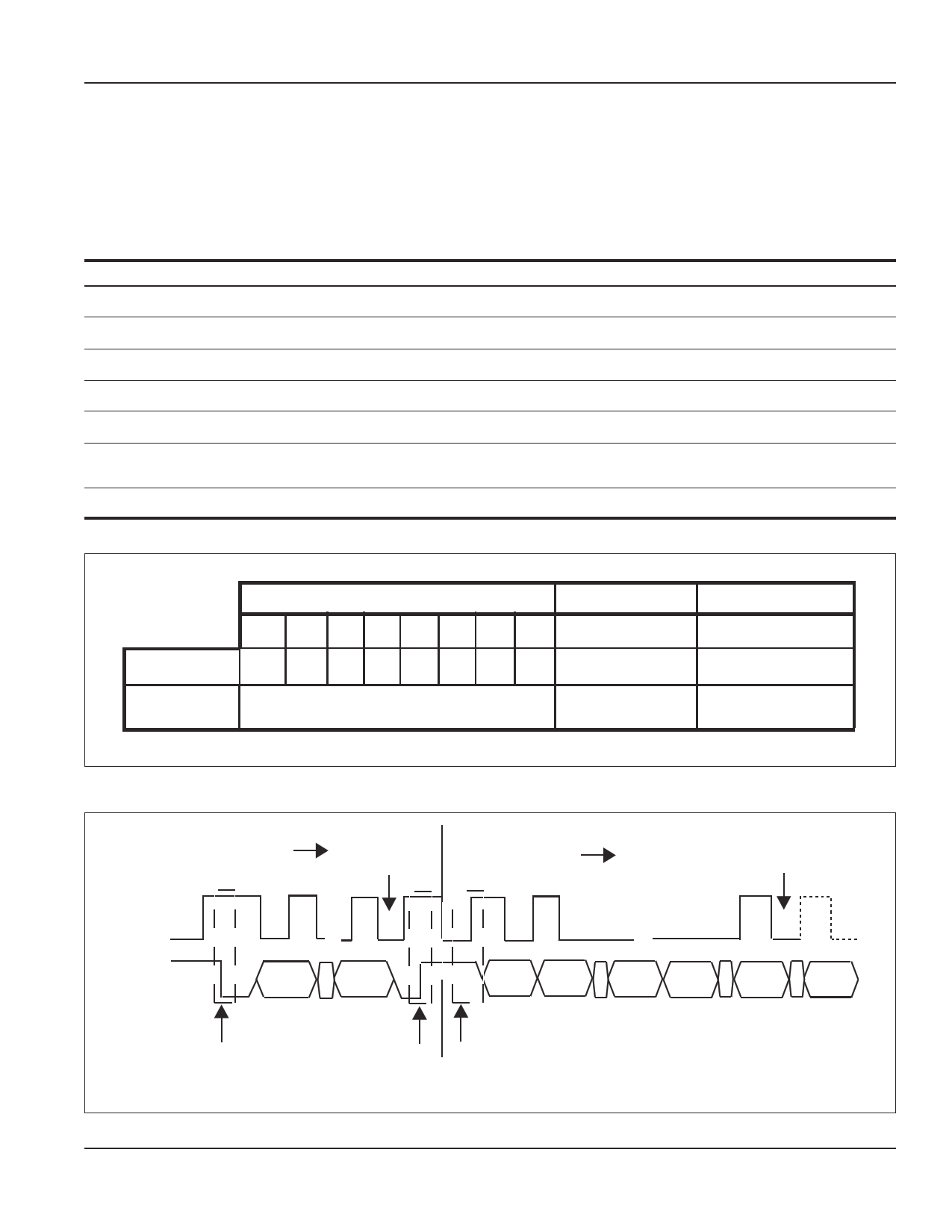
The three bytes of reference data can only be read after
successful PSC verification; otherwise, the output of the
PSC will be suppressed and the I/O will be set to the low
level. The error counter can always be read. The read
out four bytes security memory requires 32 clock pulses,
I/O is set to the high level by an additional pulse.
Address (decimal)
255
:
32
31
:
1
0
Main Memory
Data Byte 255 (D7 ...D0)
:
Data Byte 32 (D7 ... D0)
Data Byte 31(D7 ... D0)
:
Data Byte 1 (D7 ... D0)
Data Byte 0 (D7 ... D0)
Protection Memory
—
—
—
Protection Bit 31 (D31)
:
Protection Bit 1 (D1)
Protection Bit 0 (D0)
Security Memory
—
—
—
—
—
Reference Data Byte 1
(D7...D0)
Error Counter
Control
B7 B6 B5 B4 B3 B2 B1 B0
Binary
0 0 1100 01
Hexadecimal
31H
Address
A7... A0
No Effect
No Effect
Data
D7... D0
No Effect
No Effect
Command
IFD set I/O
to level L
Outgoing Data
IC sets I/O
To Level Z
01
2244
CLK ...
I/O
B0 .. X
01
...
32
D0 D1 .. D8 D9 .. D24 .. D31
Start
from IFD
Stop
from IFD
Data of
Error Counter
Start of
Outgoing Data
Reference
Data Byte 1
Reference
Data byte 3
Figure: Read Security Memory
Integrated Silicon Solution, Inc. — www.issi.com — 1-800-379-4774
Rev. 00B
08/01/03
11
11 Page | ||
| Páginas | Total 21 Páginas | |
| PDF Descargar | [ Datasheet IS23SC4442.PDF ] | |
Hoja de datos destacado
| Número de pieza | Descripción | Fabricantes |
| IS23SC4442 | 256 BYTE EEPROM | ISSI |
| Número de pieza | Descripción | Fabricantes |
| SLA6805M | High Voltage 3 phase Motor Driver IC. |
Sanken |
| SDC1742 | 12- and 14-Bit Hybrid Synchro / Resolver-to-Digital Converters. |
Analog Devices |
|
DataSheet.es es una pagina web que funciona como un repositorio de manuales o hoja de datos de muchos de los productos más populares, |
| DataSheet.es | 2020 | Privacy Policy | Contacto | Buscar |
