|
|
|
PDF TS4997 Data sheet ( Hoja de datos )
| Número de pieza | TS4997 | |
| Descripción | 2 x 1W differential input stereo audio amplifier | |
| Fabricantes | STMicroelectronics | |
| Logotipo | ||
Hay una vista previa y un enlace de descarga de TS4997 (archivo pdf) en la parte inferior de esta página. Total 30 Páginas | ||
|
No Preview Available !
www.DataSheet4U.com
TS4997
2 x 1W differential input stereo audio amplifier
with programmable 3D effects
Features
■ Operating range from VCC= 2.7V to 5.5V
■ 1W output power per channel @ VCC=5V,
THD+N=1%, RL=8Ω
■ Ultra low standby consumption: 10nA typ.
■ 80dB PSRR @ 217Hz with grounded inputs
■ High SNR: 106dB(A) typ.
■ Fast startup time: 45ms typ.
■ Pop&click-free circuit
■ Dedicated standby pin per channel
■ Lead-free QFN16 4x4mm package
Applications
■ Cellular mobile phones
■ Notebook and PDA computers
■ LCD monitors and TVs
■ Portable audio devices
Description
The TS4997 is designed for top-class stereo
audio applications. Thanks to its compact and
power-dissipation efficient QFN16 package with
exposed pad, it suits a variety of applications.
With a BTL configuration, this audio power
amplifier is capable of delivering 1W per channel
of continuous RMS output power into an 8Ω load
@ 5V.
3D effects enhancement is programmed through
a two digital input pin interface that allows more
flexibility on each output audio sound channel.
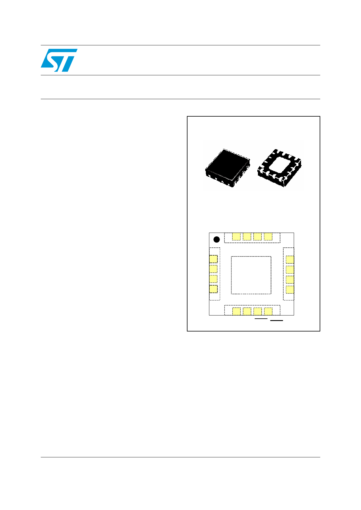
QFN16 4x4mm
Pin connections (top view)
3D0 3D1 BYP VCC
16 15 14 13
LIN-
LIN+
1
2
RIN+ 3
RIN- 4
12 LOUT-
11 LOUT+
10 ROUT+
9 ROUT-
56 78
GND GND STBYR STBYL
Each output channel (left and right), also has its
own external controlled standby mode pin to
reduce the supply current to less than 10nA per
channel. The device also features an internal
thermal shutdown protection.
The gain of each channel can be configured by
external gain setting resistors.
February 2007
Rev 2
1/34
www.st.com
34
1 page 
TS4997
3 Electrical characteristics
Electrical characteristics
Table 4.
Symbol
VCC = +5V, GND = 0V, Tamb = 25°C (unless otherwise specified)
Parameter
Min. Typ.
Max.
Unit
ICC
Supply current
No input signal, no load, left and right channel active
7.4 9.6
ISTBY
Standby current (1)
No input signal, VSTBYL = GND, VSTBYR = GND, RL = 8Ω
10 2000
Voo
Output offset voltage
No input signal, RL = 8Ω
1 35
Po
Output power
THD = 1% Max, F = 1kHz, RL = 8Ω
800 1000
THD + N
PSRR
Total harmonic distortion + noise
Po = 700mWrms, G = 6dB, RL = 8Ω, 20Hz ≤ F ≤ 20kHz
Power supply rejection ratio(2), inputs grounded
RL = 8Ω, G = 6dB, Cb = 1µF, Vripple = 200mVpp, 3D effect off
F = 217Hz
F = 1kHz
0.5
80
75
mA
nA
mV
mW
%
dB
CMRR
Common mode rejection ratio(3)
RL = 8Ω, G = 6dB, Cb = 1µF, Vincm = 200mVpp, 3D effect off
F = 217Hz
F = 1kHz
57
57
dB
SNR
Signal-to-noise ratio
A-weighted, G = 6dB, Cb = 1µF, RL = 8Ω, 3D effect off
(THD + N ≤ 0.5%, 20Hz < F < 20kHz)
108 dB
Channel separation, RL = 8Ω, G = 6dB, 3D effect off
Crosstalk F = 1kHz
F = 20Hz to 20kHz
105 dB
80
VN
Gain
Output voltage noise, F = 20Hz to 20kHz, RL = 8Ω, G=6dB
Cb = 1µF, 3D effect off
Unweighted
A-weighted
Gain value (RIN in kΩ)
4-----0-----k---Ω--
RIN
15
10
5-----0-----k---Ω--
RIN
6-----0-----k---Ω--
RIN
μVrms
V/V
tWU Wake-up time (Cb = 1µF)
46 ms
tSTBY Standby time (Cb = 1µF)
10 µs
ΦM
Phase margin at unity gain
RL = 8Ω, CL = 500pF
65 Degrees
GM Gain margin, RL = 8Ω, CL = 500pF
15 dB
GBP Gain bandwidth product, RL = 8Ω
1.5 MHz
1. Standby mode is active when VSTBY is tied to GND.
2. Dynamic measurements - 20*log(rms(Vout)/rms(Vripple)). Vripple is the sinusoidal signal superimposed upon VCC.
3. Dynamic measurements - 20*log(rms(Vout)/rms(Vincm)).
5/34
5 Page 
TS4997
Electrical characteristics
Figure 14. THD+N vs. frequency
10
RL = 4Ω
G = +6dB
Cb = 1μF
BW < 125kHz
1 Tamb = 25°C
Vcc=5V
Pout=950mW
Vcc=3.3V
Pout=430mW
Figure 15. THD+N vs. frequency
10
RL = 4Ω
G = +12dB
Cb = 1μF
BW < 125kHz
1 Tamb = 25°C
Vcc=5V
Pout=950mW
Vcc=3.3V
Pout=430mW
0.1
0.01
Vcc=2.7V
Pout=260mW
100 1000
Frequency (Hz)
10000
0.1
0.01
Vcc=2.7V
Pout=260mW
100 1000
Frequency (Hz)
10000
Figure 16. THD+N vs. frequency
10
RL = 8Ω
G = +6dB
Cb = 1μF
BW < 125kHz
1 Tamb = 25°C
0.1
Vcc=5V
Pout=700mW
Vcc=3.3V
Pout=300mW
Vcc=2.7V
Pout=200mW
Figure 17. THD+N vs. frequency
10
RL = 8Ω
G = +12dB
Cb = 1μF
BW < 125kHz
1 Tamb = 25°C
0.1
Vcc=5V
Pout=700mW
Vcc=3.3V
Pout=300mW
Vcc=2.7V
Pout=200mW
0.01
100 1000
Frequency (Hz)
10000
0.01
100 1000
Frequency (Hz)
10000
Figure 18. THD+N vs. frequency
10
RL = 16Ω
G = +6dB
Cb = 1μF
BW < 125kHz
1 Tamb = 25°C
0.1
Vcc=5V
Pout=450mW
Vcc=3.3V
Pout=200mW
Vcc=2.7V
Pout=120mW
Figure 19. THD+N vs. frequency
10
RL = 16Ω
G = +12dB
Cb = 1μF
BW < 125kHz
1 Tamb = 25°C
0.1
Vcc=5V
Pout=450mW
Vcc=3.3V
Pout=200mW
Vcc=2.7V
Pout=120mW
0.01
100 1000
Frequency (Hz)
10000
0.01
100 1000
Frequency (Hz)
10000
11/34
11 Page | ||
| Páginas | Total 30 Páginas | |
| PDF Descargar | [ Datasheet TS4997.PDF ] | |
Hoja de datos destacado
| Número de pieza | Descripción | Fabricantes |
| TS4990 | 1W AUDIO POWER AMPLIFIER WITH ACTIVE LOW STANDBY MODE | STMicroelectronics |
| TS4994 | 1W Differential Input/Output Audio Power Amplifier | STMicroelectronics |
| TS4995 | 1.2 W fully differential audio power amplifier | STMicroelectronics |
| TS4997 | 2 x 1W differential input stereo audio amplifier | STMicroelectronics |
| Número de pieza | Descripción | Fabricantes |
| SLA6805M | High Voltage 3 phase Motor Driver IC. |
Sanken |
| SDC1742 | 12- and 14-Bit Hybrid Synchro / Resolver-to-Digital Converters. |
Analog Devices |
|
DataSheet.es es una pagina web que funciona como un repositorio de manuales o hoja de datos de muchos de los productos más populares, |
| DataSheet.es | 2020 | Privacy Policy | Contacto | Buscar |