|
|
|
PDF KGL4125GW Data sheet ( Hoja de datos )
| Número de pieza | KGL4125GW | |
| Descripción | 10.7 GBPS ea Modulator Driver ic | |
| Fabricantes | Oki Semiconductor | |
| Logotipo | ||
Hay una vista previa y un enlace de descarga de KGL4125GW (archivo pdf) en la parte inferior de esta página. Total 6 Páginas | ||
|
No Preview Available !
www.DataSheet4U.com
1Electronic Components
August 16, 2002
GTD-18481 Rev. 4.0
KGL4125HW/GW
Preliminary
10.7 Gbps EA Modulator Driver IC
FEATURES
• Low Power
• Input Interface
• High Sensitive Input
• Output Amplitude Control
• X-Point Controllability
• Maximum Output Offset
• Logic Inversion Function
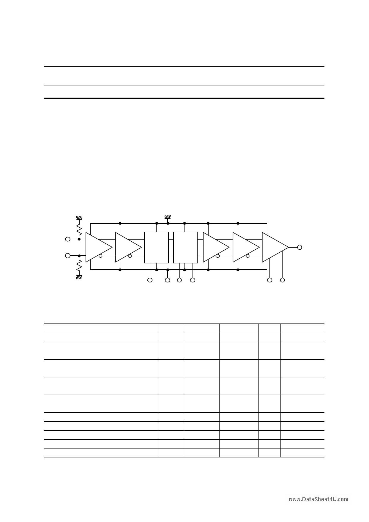
FUNCTION DIAGRAM
: 0.8 W (@minimum amplitude, no offset )
: CML Compatible / AC coupled
: 0.15 Vpp (differential)
: 0.8 Vpp to 2.3 Vpp
: 35 % to 80 %
: 1.3 V ( @50Ω )
INB
Logic
Crossing
Point
Inversion Control
IN
OUT
VPN VS VB1 VB2
VC1 VC2
ABSOLUTE MAXIMUM RATINGS
Parameter
Supply Voltage
X-Point Control Voltage
X-Point Reference Voltage
Output Amplitude Control Voltage
Symbol
VS
VB1
VB2
Min
-6.5
VS-5.0
(Min. -6.5)
VS-5.0
(Min. -6.5)
VC1 -6.5
Output Bias Control Voltage
Logic Inversion Control Voltage
Input Voltage
Input Amplitude
Operating Temperature at Package Base
Storage Temperature
VC2
VPN
Vin(DC)
Vin
Ts
Tst
-6.5
-6.5
-2
-
-10
-40
Max
0.3
VS+3.0
(Max. 0.3)
VS+3.0
(Max. 0.3)
VS+1.6
(Max. 0.3)
VS+2.6
(Max. 0.3)
0.3
0.6
1.5
100
125
Unit Note
V
V
V
V
V
V
V DC coupled
Vpp AC coupled
°C
°C
1/6
1 page 
www.DataSheet4U.com
1Electronic Components
TYPICAL APPLICATION
GTD-18481 Rev. 4.0
KGL4125HW/GW
VPN GND
KGL4125HW/GW
Data-bar Input
INB
Data Input
IN
Blocking
Capacitor
Ex. 0.1µF
50Ω
OUT
VB1 VB2 VS VC1 VC2
EAM
Chip
Capacitor
≥ 0.1µF
APPLICATION NOTE
1. For stable operation;
1-1. To prevent a dependence of “X-Point” on the supply voltage VS,
(1) Use an external voltage source of –3.8V for “VB2”, or
(2) Control the voltage of “VB1”, so that the voltage difference “VB1– VB2” is constant.
1-2. To prevent a dependence of “Output amplitude” on the supply voltage VS,
Control the voltage of “VC1”, so that the voltage difference “VC1– VS” is constant.
1-3. To prevent a dependence of “Output bias control voltage” on supply voltage VS,
Control the voltage of “VC2”, so that the voltage difference “VC2– VS” is constant.
2. Power-up/shut-down sequence;
For power-up, supply control voltages (VB1, (VB2), VC1, VC2) at first, then Vs
or supply all simultaneously.
For shut-down, Vs at first, then control voltages or shut down all simultaneously. .
Customer does not need to care about the sequence for the control voltages (VB1,(VB2),VC1,VC2).
5/6
5 Page | ||
| Páginas | Total 6 Páginas | |
| PDF Descargar | [ Datasheet KGL4125GW.PDF ] | |
Hoja de datos destacado
| Número de pieza | Descripción | Fabricantes |
| KGL4125GW | 10.7 GBPS ea Modulator Driver ic | Oki Semiconductor |
| Número de pieza | Descripción | Fabricantes |
| SLA6805M | High Voltage 3 phase Motor Driver IC. |
Sanken |
| SDC1742 | 12- and 14-Bit Hybrid Synchro / Resolver-to-Digital Converters. |
Analog Devices |
|
DataSheet.es es una pagina web que funciona como un repositorio de manuales o hoja de datos de muchos de los productos más populares, |
| DataSheet.es | 2020 | Privacy Policy | Contacto | Buscar |