|
|
|
PDF ML145053 Data sheet ( Hoja de datos )
| Número de pieza | ML145053 | |
| Descripción | 10-Bit A/D Converter | |
| Fabricantes | LANSDALE Semiconductor | |
| Logotipo | ||
Hay una vista previa y un enlace de descarga de ML145053 (archivo pdf) en la parte inferior de esta página. Total 15 Páginas | ||
|
No Preview Available !
www.DataSheet4U.com
ML145053
10-Bit A/D Converter With
Serial Interface
CMOS
Legacy Device: Motorola MC145053
This ratiometric 10-bit ADC has a serial interface port to provide commu-
nication with MCUs and MPUs. Either a 10- or 16-bit format can be used.
The16-bit format can be one continuous 16-bit stream or two intermittent 8-
bit streams. The converter operates from a single power supply with no exter-
nal trimming required. Reference voltages down to 4.0 V are accommodated.
The ML145053 has an internal clock oscillator to operate the dynamic A/D
conversion sequence and an end-of-conversion (EOC) output.
• 5 Analog Input Channels with Internal Sample-and-Hold
• Operating Temperature Range: TA – 40 to 125°C
• Successive Approximation Conversion Time: 44 µs Maximum
• Maximum Sample Rate: 20.4 ks/s
• Analog Input Range with 5-Volt Supply: 0 to 5 V
• Monotonic with No Missing Codes
• Direct Interface to Motorola SPI and National MICROWIRE™
Serial DataPorts
• Digital Inputs/Outputs are TTL, NMOS, and CMOS Compatible
• Low Power Consumption: 14 mW
• Chip Complexity: 1630 Elements (FETs, Capacitors, etc.)
• See Application Note AN1062 for Operation with QSPI
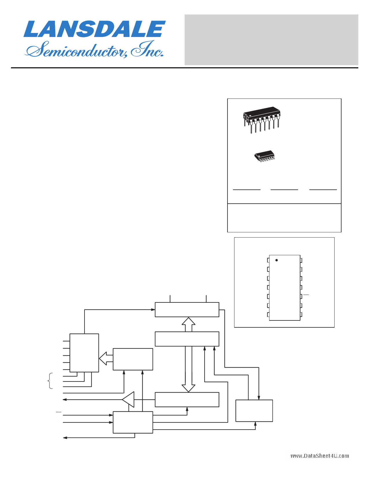
BLOCK DIAGRAM
MUX OUT
Vref VAG
98
10–BIT RC DAC
WITH SAMPLE AND HOLD
P DIP 14 = CP
PLASTIC
CASE 646
SOG 14 = -5P
SOG
CASE 751A
CROSS REFERENCE/ORDERING INFORMATION
PACKAGE
MOTOROLA
LANSDALE
P DIP 14
SOG 14
MC145053P ML145053CP
MC145053D ML145053-5P
Note: Lansdale lead free (Pb) product, as it
becomes available, will be identified by a part
number prefix change from ML to MLE.
PIN ASSIGNMENT
EOC 1
AN0 2
AN1 3
AN2 4
AN3 5
AN4 6
VSS 7
14 VDD
13 SCLK
12 Din
11 Dout
10 CS
9 Vref
8 VAG
INTERNAL
TEST
VOLTAGES
AN0 2
AN1 3
AN2 4
AN3 5
AN4 6
ANALOG
MUX
AN5
AN6
AN7
Din 12
Dout 11
SUCCESSIVE APPROXIMATION
REGISTER
MUX ADDRESS
REGISTER
DATA REGISTER
CS 10
SCLK 13
EOC 1
DIGITAL CONTROL
LOGIC
MICROWIRE is a trademark of National Semiconductor Corp.
Page 1 of 15
www.lansdale.com
PIN 14 = VDD
PIN 7 = VSS
AUTO–ZEROED
COMPARATOR
Issue A
1 page 
ML145053
www.DataSheet4U.com
LANSDALE Semiconductor, Inc.
tf
2.0 V
SCLK
Dout
tWL tWH
tr
0.8 V
1/f
tPLH, tPHL
2.4 V
0.4 V
tTLH, tTHL
Figure 1.
SWITCHING WAVEFORMS
CS
Dout
0.8 V
tPZH, tPZL
2.4 V
0.4 V
2.0 V
tPHZ, tPLZ
90%
10%
Figure 2.
Din
SCLK
VALID
2.0 V
0.8 V
tsu
th
2.0 V
0.8 V
Figure 3.
EOC 0.4 V
tTLH
2.4 V
td
Dout
2.4 V
0.4 V
VALID MSB
NOTE: Dout is driven only when CS is active (low).
Figure 4.
CS
SCLK
0.8 V
tsu
FIRST
0.8 V CLOCK
Figure 5.
2.0 V
th
LAST
CLOCK 0.8 V
VDD
TEST
POINT
Dout
DEVICE
UNDER
TEST
12 k 100 pF
SCLK
EOC
10TH
CLOCK
0.8 V
2.4 V
tTHL
tPHL
0.4 V
Figure 6.
VDD
TEST
POINT
EOC
DEVICE
UNDER
TEST
12 k 50 pF
Page 5 of 15
Figure 7. Test Circuit
www.lansdale.com
Figure 8. Test Circuit
Issue A
5 Page 
ML145053
www.DataSheet4U.com
LANSDALE Semiconductor, Inc.
Legacy Applications Information
DESCRIPTION
This example application of the ML145053 ADC interfaces
four analog signals to a microprocessor.
Figure 15 illustrates how the ML145053 is used as a cost
effective means to simplify this type of circuit design. Utilizing
one ADC, four analog inputs are interfaced to a CMOS or
NMOS microprocessor with a serial peripheral interface (SPI)
port. Processors with National Semiconductor's MICROWIRE
serial port may also be used. Full duplex operation optimizes
throughput for this system.
DIGITAL DESIGN CONSIDERATIONS
Motorola's MC68HC05C4 CMOS MCU may be chosen to
reduce power supply size and cost. The NMOS MCUs may be
used if power consumption is not critical. A VDD or VSS 0.1
µF bypass capacitor should be closely mounted to the ADC.
The ML145053 has the end-of-conversion (EOC) signal at
output pin 1 to define when data is ready.
ANALOG DESIGN CONSIDERATIONS
Analog signal sources with output impedances of less than
1 kΩ may be directly interfaced to the ADC, eliminating the
need for buffer amplifiers. Separate lines connect the Vref and
VAG pins on the ADC with the controllers to provide isolation
from system noise.
Although not indicated in Figure 15, the Vref and sensor out-
put lines may need to be shielded, depending on their length
and electrical environment. This should be verified during pro-
totyping with an oscilloscope. If shielding is required, a twist-
ed pair or foil-shielded wire (not coax) is appropriate for this
low frequency application. One wire of the pair or the shield
must be VAG.
A reference circuit voltage of 5 volts is used for the applica-
tion shown in Figure 15. However, the reference circuitry may
be simplified by tying VAG to system ground and Vref to the
system's positive supply. (See Figure 16.)
A bypass capacitor of approximately 0.22 µF across theVref
and VAG pins is recommended. These pins are adjacent on the
ADC package which facilitates mounting the capacitor very
close to the ADC.
SOFTWARE CONSIDERATIONS
The software flow for acquisition is straight forward. The
four analog inputs, AN0 through AN3, are scanned by reading
the analog value of the previously addressed channel into the
MCU and sending the address of the next channel to be read to
the ADC, simultaneously.
The designer utilizing the ML145053 has the end-of-con-
version signal (at pin 1) to define the conversion interval. EOC
may be used to generate an interrupt, which is serviced by
reading the serial data from the ADC. The software flow
should then process and format the data.
When this ADC is used with a 16-bit (2-byte) transfer, there
are two types of offsets involved. In the first type of offset, the
channel information sent to the ADCs is offset by 12 bits. That
is, in the 16-bit stream, only the first 4 bits (4 MSBs) contain
the channel information. The balance of the bits are don't
cares. This results in 3 don't-care nibbles, as shown in Table 2.
The second type of offset is in the conversion result returned
from the ADC; this is offset by 6 bits. In the 16-bitstream, the
first 10 bits (10 MSBs) contain the conversion result. The last
6 bits are zeroes. The hexadecimal result is shown in the first
column of Table 3. The second column shows the result after
the offset is removed by a micro-processor routine. If the 16-
bit format is used, the ADC can transfer one continuous 16-bit
stream or two intermittent 8-bitstreams.
Page 11 of 15
www.lansdale.com
Issue A
11 Page | ||
| Páginas | Total 15 Páginas | |
| PDF Descargar | [ Datasheet ML145053.PDF ] | |
Hoja de datos destacado
| Número de pieza | Descripción | Fabricantes |
| ML145050 | (ML145050 / ML145051) 10-Bit A/D Converter | LANSDALE Semiconductor |
| ML145051 | (ML145050 / ML145051) 10-Bit A/D Converter | LANSDALE Semiconductor |
| ML145053 | 10-Bit A/D Converter | LANSDALE Semiconductor |
| Número de pieza | Descripción | Fabricantes |
| SLA6805M | High Voltage 3 phase Motor Driver IC. |
Sanken |
| SDC1742 | 12- and 14-Bit Hybrid Synchro / Resolver-to-Digital Converters. |
Analog Devices |
|
DataSheet.es es una pagina web que funciona como un repositorio de manuales o hoja de datos de muchos de los productos más populares, |
| DataSheet.es | 2020 | Privacy Policy | Contacto | Buscar |