|
|
|
PDF GD16588 Data sheet ( Hoja de datos )
| Número de pieza | GD16588 | |
| Descripción | (GD16584 / GD16588) Receiver / CDR and DeMUX | |
| Fabricantes | Giga | |
| Logotipo | ||
Hay una vista previa y un enlace de descarga de GD16588 (archivo pdf) en la parte inferior de esta página. Total 15 Páginas | ||
|
No Preview Available !
www.DataSheet4U.com
an Intel company
10 Gbit/s
Receiver, CDR and
DeMUX
GD16584/GD16588
(FEC)
Preliminary
General Description
Features
GD16584 and GD16588 are Receiver
chips for use in STM-64/192 and Optical
Transport Networking (OTN) systems.
The component is available in two ver-
sions:
u GD16584 for 9.5328 Gbit/s.
u GD16588 for 10.66 Gbit/s for OTN or
Forward Error Correction (FEC).
Except the different operating bit rates
the two versions are functional identical.
The receiver is a Clock and Data Reco-
very IC with:
u a low noise VCO
u a Bang-Bang Phase Detector
u a 1:16 De-multiplexer
u a Lock Detect
u a Phase and Frequency Detector.
Clock and data are regenerated by using
a Phase Locked Loop (PLL) with an ex-
ternal passive loop filter.
The VCO frequency is controlled by one
of the two Phase Detectors in order to
ensure capture and lock to the line data
rate. The Lock Detector circuit monitors
the VCO frequency and determines when
the VCO is within the lock range. When
the frequency deviates more than
500 ppm from the reference clock, it
automatically switches the phase and fre-
quency detector into the PLL loop. In the
auto lock mode the locking range is
selectable between 500 or 2000 ppm.
When the VCO frequency is within the
lock range, the Bang-Bang Phase Detec-
tor takes over. It controls the phase of
the VCO until the sampling point of data
is in the middle of the bit period, where
the eye opening is largest. A ±40 mV
Decision Threshold Control (DTC) is pro-
vided at the 10 Gbit/s input.
The 10 Gbit/s input data is sampled and
de-multiplexed by the 1:16 DeMUX. The
parallel output interface is synchronised
with the 622 MHz output clock. The clock
and data outputs are LVDS compatible.
The device operates from a dual -5.2 V
and +3.3 V power supply. The power dis-
sipation is 3.3 W, typical.
The device is manufactured in a Silicon
Bipolar process and packaged in an 132
ball 13 × 13 mm Ceramic/Plastic Ball
Grid Array (BGA).
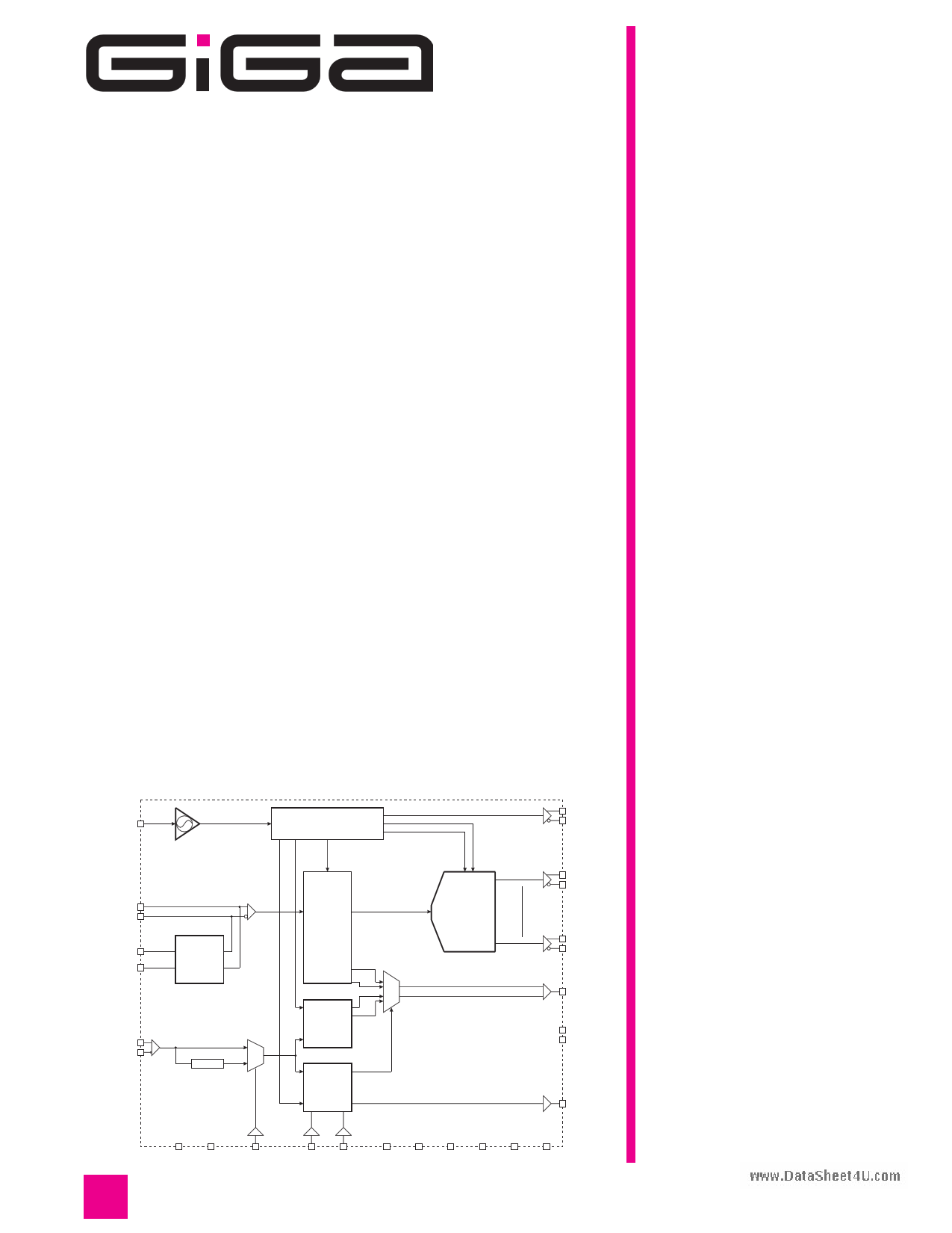
VCTL
VCO
Timing Control
CKOUT
CKOUTN
DI
DIN
DTC
DTCN
Decision
Threshold
Control
REFCK
REFCKN
1/4
Bang
Bang
Phase
Detector
Phase
Frequency
Detector
Lock
Detect
1:16
Demultiplexer
U
D
Parallel
Output
Data
DO0
DON0
DO15
DON15
PCTL
(PHIGH)
(PLOW)
LOCK
RESET TCK
SEL3
SEL1 SEL2
VCC VDD VDDA VDDO VEE VEEA
l Complete Clock and Data Recovery
IC with auto acquisition.
l 1:16 DeMUX with differential
622 Mbit/s data outputs
l 622 MHz Clock output.
l LVDS compatible clock and data
outputs.
l OIF99.102.5 compliant timing.
l 155 or 622 MHz Reference Clock.
l Input Decision Threshold Control
(DTC): ±40 mV.
l Low noise VCO with ±5 % tuning
range.
l Dual supply operation: -5.2 V and
+3.3 V.
l Power dissipation: 3.3 W (typ).
l Silicon Bipolar technology.
l Available in three package versions:
– EB: 132 ball (16 mill) Ceramic
BGA 13 × 13 mm
– EF: 132 ball (20 mill) Ceramic
BGA 13 × 13 mm
– FB: 132 ball (20 mill) Plastic
BGA 13 × 13 mm
l Available in two versions:
– GD16584 for 10 Gbit/s
– GD16588 for 10.66 Gbit/s
Applications
l Telecommunication systems:
– SDH STM-64
– SONET OC-192.
– Optical Transport Networking
(OTN)
– FEC applications
l Fibre optic test equipment.
l Submarine systems.
Data Sheet Rev.: 12
1 page 
www.DAatapShpeelti4cUa.cotmions Continued
10 Gbit/s Input Interface
Postamplifier
0V
50W
GD16584/GD16588
0V
50W 50W
0/-0.4V
0/-0.4V
50W MSL
DI
DIN
>16mA
-5.2V
Figure 3. 10 Gbit/s Input (DI/DIN), DC Coupled
Post-
amplifier
GD16584/GD16588
0V
-5.2V
50W
50W
220W
DI
50W MSL 100nF DIN
220W
-5.2V
-5.2V
Figure 4. 10 Gbit/s Input (DI/DIN), AC Coupled
Data Sheet Rev.: 12
GD16584/GD16588
Page 5 of 15
5 Page 
www.DDataCSheCet4hUa.cormacteristics
TCASE* = 0 °C to 70 °C. VEE = -5.2 V, VCC = +3.3 V. VDD is 0 V or GND.
All voltages in table are referred to VDD.
All currents are defined positive out of pin.
Symbol:
VEE
IEE
VCC
ICC
VOH LVDS
VOL LVDS
VOD LVDS
VIH CML
VIL CML
IIH CML
IIL CML
RIN CML
IOH OC
IOL OC
VIH ECL
VIL ECL
IIH ECL
IIL ECL
VADS
Characteristic:
Negative Supply Voltage
Negative Supply Current
Positive Supply Voltage
Positive Supply Current
LVDS Output Voltage High
LVDS Output Voltage Low
LVDS Output Differential Voltage
CML Input Voltage High
CML Input Voltage Low
CML Input Current High
CML Input Current Low
CML Input Resistor Termination
Open Collector Output Current High
Open Collector Output Current Low
ECL Input Voltage High
ECL Input Voltage Low
ECL Input Current High
ECL Input Current Low
Offset Adjustment by DTC/DTCN, Differential
Conditions:
Note 7, VCC = 3.3 V
Note 7, VCC = 3.3 V
Note 7, VCC = 3.3 V
VIH CML, 50 W input
VIL CML, 50 W input
DC
Note 1, 3
Note 1, 3
Note 2, 5
Note 2, 5
V = -1.1 V
V = -1.5 V
Note 4, 6
MIN.:
-5.46
455
3.135
-180
0.9
250
-0.1
-1
40
-0.1
-10
-1.1
VEE
TYP.:
-5.2
550
3.3
-140
1.4
1.1
400
0
-0.4
0
8
50
0
-8
±90
Note 1:
Note 2:
Note 3:
Note 4:
Note 5:
Note 6:
Note 7:
Output externally terminated by 50 W to 0 V.
All ECL inputs can be connected directly to VDD/VEE.
All open collector outputs should always be terminated with a resistor.
With DTC and DTCN connected to a 10k potentiometer with the mid pin grounded (0 V).
-5.0 V.
With open data inputs.
With 100 W termination resistor.
*: TCASE measured at the center of the top.
MAX.:
-4.94
660
3.465
1.5
600
+0.1
-0.25
60
+0.1
-7
0
-1.5
30
30
UNIT:
V
mA
V
mA
V
V
mV
V
V
mA
mA
W
mA
mA
V
V
mA
mA
mV
Data Sheet Rev.: 12
GD16584/GD16588
Page 11 of 15
11 Page | ||
| Páginas | Total 15 Páginas | |
| PDF Descargar | [ Datasheet GD16588.PDF ] | |
Hoja de datos destacado
| Número de pieza | Descripción | Fabricantes |
| GD16584 | (GD16584 / GD16588) Receiver / CDR and DeMUX | Giga |
| GD16585 | (GD16585 / GD16589) Transmitter MUX | Giga |
| GD16585 | Transmitter MUX | Giga |
| GD16588 | (GD16584 / GD16588) Receiver / CDR and DeMUX | Giga |
| Número de pieza | Descripción | Fabricantes |
| SLA6805M | High Voltage 3 phase Motor Driver IC. |
Sanken |
| SDC1742 | 12- and 14-Bit Hybrid Synchro / Resolver-to-Digital Converters. |
Analog Devices |
|
DataSheet.es es una pagina web que funciona como un repositorio de manuales o hoja de datos de muchos de los productos más populares, |
| DataSheet.es | 2020 | Privacy Policy | Contacto | Buscar |