|
|
PDF AT40KFL040 Data sheet ( Hoja de datos )
| Número de pieza | AT40KFL040 | |
| Descripción | Rad Hard Reprogrammable FPGAs | |
| Fabricantes | ATMEL Corporation | |
| Logotipo |  |
|
Hay una vista previa y un enlace de descarga de AT40KFL040 (archivo pdf) en la parte inferior de esta página. Total 30 Páginas | ||
|
No Preview Available !
Features
• SRwAwMwb.DaastaeSdhFeePtG4UA.cDomedicated to Space Use
• SEE Hardened Cells (configuration RAM, FreeRAM, DFF, JTAG, I/O buffers) Remove the
need for Triple Modular Redundancy (TMR)
• Produced on Rad Hard 0.35µm CMOS Process
• Functionally and Pin Compatible with the Atmel Commercial and Military AT40K Series
• High Performance
– 46K Available ASIC gates (50% typ. routable)
– 60 MHz Internal Performance
– 20 MHz System Performance
– 30 MHz Array Multipliers
– 18 ns FreeRAM™ access time
– Internal Tri-state Capability in Each Cell
• FreeRAM
– 18432 Bits of Distributed SRAM Independent of Logic Cells
– Flexible, Single/Dual Port, Synchronous/Asynchronous 32x4 RAM blocks
• 8 Global Clocks and 4 Additional Dedicated PCI Clocks
– Fast, Low Skew Clock Distribution
– Programmable Rising/Falling Edge Transitions
– Distributed Clock Shutdown Capability for Low Power Management
• Global Reset Option
• 384 PCI Compliant I/Os
– Programmable Output Drive
– Fast, Flexible Array Access Facilitates Pin Locking
• Package Options
– MQFPF160
– MQFPF256
• Design Software (System Designer)
– Combination of Atmel internally developed tools, and industry standard design
tools
– Fast and Efficient Synthesis
– Efficient Integration (Libraries, Interface, Full Back-annotation)
– Over 75 Automatic Component Generators Create Thousands
of Speed and Area Optimized Logic and RAM Functions
– Automatic/Interactive Multi-chip Partitioning
• Supply Voltage 3.3V
• AT40KFL040 is a 5V Tolerant Version
• No Single Event Latch-up below a LET Threshold of 70 MeV/mg/cm2
• Tested up to a Total Dose of 300 krads (Si) according to MIL STD 883 Method 1019
• Quality Grades
– QML -Q and -V with SMD 5962-03250
– ESCC with 9304/008
• Design Kit (AT40KEL-DK) Including:
– A Board with the RH FPGA (MQFPF160 or MQFPF256)
– A configuration memory (AT17 Atmel EEPROM)
– Design software and documentation
– ISP cable and software
• Easy Migration to Atmel Gate Arrays for High Volume Production
Rad Hard
Reprogrammable
FPGAs with
FreeRAM
AT40KEL040
AT40KFL040
Note:
All features and characteristics described for
AT40KEL040 in this document, also apply to the
AT40KFL040 unless specified otherwise.
4155I–AERO–06/06
1 page 
www.DataSheet4U.com
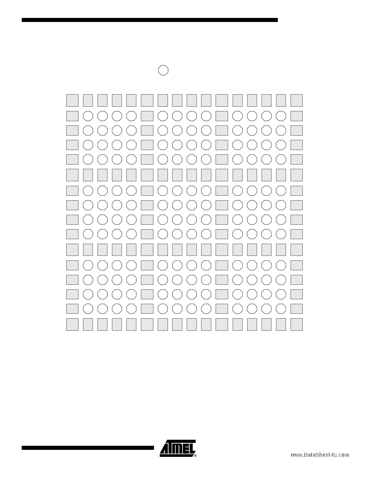
Figure 2. Floorplan (Representative Portion)(1)
= Core Cell
AT40KEL040
RAM RV RV RV RV RAM RV RV RV RV RAM RV RV RV RV RAM
RH RH RH RH
RH RH RH RH
RH RH RH RH
RH RH RH RH
RAM RV RV RV RV RAM RV RV RV RV RAM RV RV RV RV RAM
RH RH RH RH
RH RH RH RH
RH RH RH RH
RH RH RH RH
RAM RV RV RV RV RAM RV RV RV RV RAM RV RV RV RV RAM
RH RH RH RH
RH RH RH RH
RH RH RH RH
RH RH RH RH
RAM RV RV RV RV RAM RV RV RV RV RAM RV RV RV RV RAM
Note:
1. Repeaters regenerate signals and can connect any bus to any other bus (all path-
ways are legal) on the same plane. Each repeater has connections to two adjacent
local-bus segments and two express-bus segments. This is done automatically using
the integrated development system (IDS) tool.
4155I–AERO–06/06
5
5 Page 
RAM
www.DataSheet4U.com
AT40KEL040
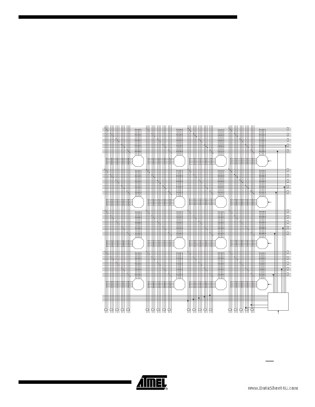
32 x 4 dual-ported RAM blocks are dispersed throughout the array as shown in Figure 7.
A 4-bit Input Data Bus connects to four horizontal local buses distributed over four sec-
tor rows (plane 1). A 4-bit Output Data Bus connects to four horizontal local buses dis-
tributed over four sector rows (plane 2). A 5-bit Input Address Bus connects to five
vertical express buses in same column. A 5-bit Output Address Bus connects to five ver-
tical express buses in same column. Ain (input address) and Aout (output address)
alternate positions in horizontally aligned RAM blocks. For the left-most RAM blocks,
Aout is on the left and Ain is on the right. For the right-most RAM blocks, Ain is on the
left and Aout is tied off, thus it can only be configured as a single port. For single-ported
RAM, Ain is the READ/WRITE address port and Din is the (bi-directional) data port.
Right-most RAM blocks can be used only for single-ported memories. WEN and OEN
connect to the vertical express buses in the same column.
Figure 7. RAM Connections (One Ram Block)
CLK
CLK
CLK
4155I–AERO–06/06
CLK
Din Dout
Ain Aout
32 x 4 RAM
WEN
OEN CLK
Reading and writing of the 18 ns 32 x 4 dual-port FreeRAM are independent of each
other. Reading the 32 x 4 dual-port RAM is completely asynchronous. Latches are
transparent; when Load is logic 1, data flows through; when Load is logic 0, data is
latched. These latches are used to synchronize Write Adress, Write Enable Not, and Din
signals for a synchronous RAM. Each bit in the 32 x 4 dual-port RAM is also a transpar-
ent latch. The front-end latch and the memory latch together form an edge-triggered flip
flop. When a nibble (bit = 7) is (Write) addressed and LOAD is logic 1 and WE is logic 0,
11
11 Page | ||
| Páginas | Total 30 Páginas | |
| PDF Descargar | [ Datasheet AT40KFL040.PDF ] | |
Hoja de datos destacado
| Número de pieza | Descripción | Fabricantes |
| AT40KFL040 | Rad Hard Reprogrammable FPGAs | ATMEL Corporation |
| Número de pieza | Descripción | Fabricantes |
| SLA6805M | High Voltage 3 phase Motor Driver IC. |
Sanken |
| SDC1742 | 12- and 14-Bit Hybrid Synchro / Resolver-to-Digital Converters. |
Analog Devices |
|
DataSheet.es es una pagina web que funciona como un repositorio de manuales o hoja de datos de muchos de los productos más populares, |
| DataSheet.es | 2020 | Privacy Policy | Contacto | Buscar |
