|
|
|
PDF ISL12032 Data sheet ( Hoja de datos )
| Número de pieza | ISL12032 | |
| Descripción | Low Power RTC | |
| Fabricantes | Intersil Corporation | |
| Logotipo | ||
Hay una vista previa y un enlace de descarga de ISL12032 (archivo pdf) en la parte inferior de esta página. Total 26 Páginas | ||
|
No Preview Available !
ISL12032
®
Real Time Clock with 50/60 Hz clock and Crystal Backup
Data Sheet
December 14, 2007
FN6618.0
Low Power RTC with Battery Backed
SRAM and 50/60 Cycle AC Input and Xtal
www.Bdaatacshke-eut4pu.com
The ISL12032 device is a low power real time clock with
50/60 AC input for timing synchronization. It also has an
oscillator utilizing an external crystal for timing back-up,
clock/calendar registers, intelligent battery back-up
switching, battery voltage monitor, brownout indicator,
integrated trickle charger for super capacitor, single periodic
or polled alarms, POR supervisory function, and up to 4
Event Detect with time stamp. There are 128 bytes of
battery-backed user SRAM.
The oscillator uses a 50/60 cycle sine wave input, backed by
an external, low-cost, 32.768kHz crystal. The real time clock
tracks time with separate registers for hours, minutes, and
seconds. The calendar registers contain the date, month,
year, and day of the week. The calendar is accurate through
year 2100, with automatic leap year correction and auto
daylight savings correction.
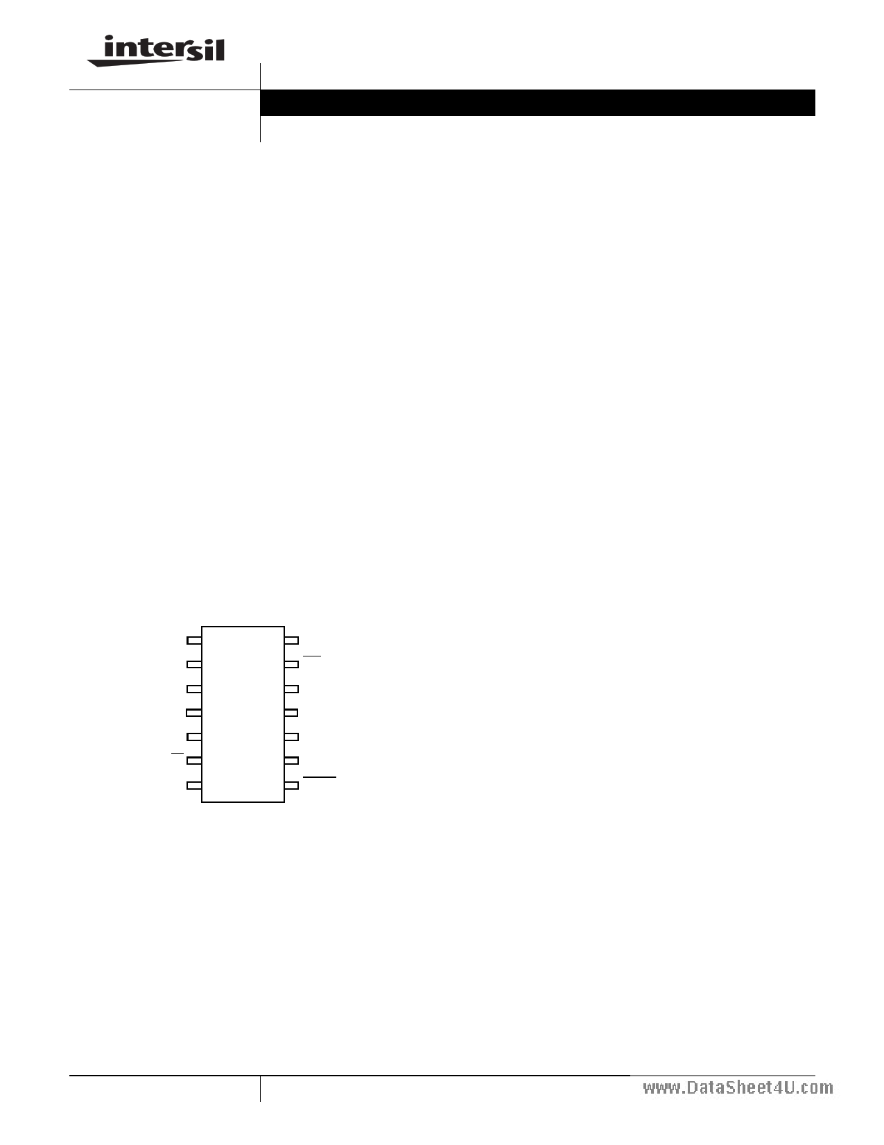
Pinout
ISL12032
(14 LD TSSOP)
TOP VIEW
X1
X2
VBAT
GND
AC
LV
EVIN
1
2
3
4
5
6
7
14 VDD
13 IRQ
12 SCL
11 SDA
10 ACRDY
9 FOUT
8 EVDET
Features
• 50/60 Cycle AC as a Primary Clock Input for RTC Timing
• Redundant Crystal Clock Input Selectable by User
- Dynamically Switch from AC Clock Input to Crystal in
Case of Power Failure
• Real Time Clock/Calendar
- Tracks Time in Hours, Minutes, Seconds and tenths of a
second
- Day of the Week, Day, Month, and Year
• Auto Daylight Saving Time Correction
- Programmable Forward and Backward Dates
• Security and Event Functions
- Event Detection with Time Stamp
- Stores First and Last Three Event Time Stamps
• Separate FOUT Pin
- 7 Selectable Frequency Outputs
• Dual Alarms with Hardware and Register Indicators
- Hardware Single Event or Pulse Interrupt Mode
• Automatic Backup to Battery or Super Capacitor
- VBAT Operation Down to 1.8V
- 1.0µA Battery Supply Current
• Two Battery Status Monitors with Selectable Levels
- Seven Selectable Voltages for Each Level
- 1st Level, Trip Points from 4.675V to 2.125V
- 2nd Level, Trip Points from 4.125V to 1.875V
• VDD Power Brownout Monitor
- Six Selectable Trip Levels, from 4.675V to 2.295V
• Time Stamp during Power to Battery and Battery to Power
Switchover
• Integrated Trickle Charger
- Four Selectable Charging Rates
• 128 Bytes Battery-Backed User SRAM
• I2C Interface
- 400kHz Data Transfer Rate
• Pb-free (RoHS compliant)
Applications
• Utility Meters
• Control Applications
• Security Related Applications
• Vending Machines
• White Goods
• Consumer Electronics
1 CAUTION: These devices are sensitive to electrostatic discharge; follow proper IC Handling Procedures.
1-888-INTERSIL or 1-888-468-3774 | Intersil (and design) is a registered trademark of Intersil Americas Inc.
Copyright Intersil Americas Inc. 2007. All Rights Reserved
All other trademarks mentioned are the property of their respective owners.
1 page 
ISL12032
DC Operating Characteristics Specifications apply for: VDD = 2.7 to 5.5V, TA = -40°C to +85°C, unless otherwise stated. (Continued)
SYMBOL
PARAMETER
CONDITIONS
MIN TYP MAX
(Note 10) (Note 4) (Note 10) UNITS NOTES
IRQ/ACRDY/LV/EVDET (OPEN DRAIN OUTPUTS)
VOL Output Low Voltage
www.datasheet4u.com
FOUT (CMOS OUTPUT)
VOL Output Low Voltage
VOH
Output High Voltage
EVIN
VDD = 5V, IOL = 3mA
VDD = 2.7V, IOL = 1mA
IOH = 1mA
0.7 x VDD
0.4 V
0.4 V
0.3 x VDD
V
V
IEVPU
VIL
VIH
IEVPD
EVIN Pull-up Current
Input Low Voltage
Input High Voltage
EVIN Disabled Pull-down Current
VDD = 5.5V, VBAT = 3.0V
VDD = 0V, VBAT = 1.8V
VDD = 5.5V
1.0
100
0.7 x VDD
3.0 8.0
600
0.3 x VDD
200
µA
nA
V
V
nA
Power-Down Timing Specifications apply for: VDD = 2.7 to 5.5V, TA = -40°C to +85°C, unless otherwise stated.
SYMBOL
PARAMETER
CONDITIONS
MIN TYP MAX
(Note 10) (Note 4) (Note 10) UNITS
VDD SR-
VDD Negative Slew Rate
10 V/ms
I2C Interface Specifications Specifications apply for: VDD = 2.7 to 5.5V, TA = -40°C to +85°C, unless otherwise stated.
NOTES
6
SYMBOL
VIL
VIH
Hysteresis
VOL
CPIN
fSCL
tIN
tAA
tBUF
tLOW
tHIGH
PARAMETER
TEST CONDITIONS
SDA and SCL Input Buffer LOW
Voltage
SDA and SCL Input Buffer HIGH
Voltage
SDA and SCL Input Buffer
Hysteresis
SDA Output Buffer LOW Voltage, VDD = 5V, IOL = 3mA
Sinking 3mA
SDA and SCL Pin Capacitance
SCL Frequency
TA = +25°C, f = 1MHz,
VDD = 5V, VIN = 0V,
VOUT = 0V
Pulse Width Suppression Time at Any pulse narrower than the
SDA and SCL Inputs
max spec is suppressed.
SCL Falling Edge to SDA Output
Data Valid
SCL falling edge crossing
30% of VDD, until SDA exits
the 30% to 70% of VDD
window.
Time the Bus Must be Free Before
the Start of a New Transmission
SDA crossing 70% of VDD
during a STOP condition, to
SDA crossing 70% of VDD
during the following START
condition.
Clock LOW Time
Measured at the 30% of VDD
crossing.
Clock HIGH Time
Measured at the 70% of VDD
crossing.
MIN
(Note 10)
-0.3
0.7 x VDD
0.05 x VDD
1300
1300
600
TYP
MAX
(Note 4) (Note 10) UNITS
0.3 x VDD V
VDD + 0.3 V
V
0.4 V
10 pF
400 kHz
50 ns
900 ns
ns
ns
ns
NOTES
5 FN6618.0
December 14, 2007
5 Page 
ISL12032
REGISTER ACCESS
The contents of the registers can be modified by performing
a byte or a page write operation directly to any register
address.
The registers are divided into 10 sections. They are:
1. Real Time Clock (8 bytes): Address 00h to 07h.
www.datasheet4u.com
2. Status (2 bytes): Address 08h to 09h.
3. Counter (2 bytes): Address Ah to Bh.
4. Control (9 bytes): 0Ch to 14h.
5. Day Light Saving Time (8 bytes): 15h to 1Ch
6. Alarm 0/1 (12 bytes):1Dh to 28h
7. Time Stamp for Battery Status (5 bytes): Address 29h to
2Dh.
8. Time Stamp for VDD Status (5 bytes): Address 2Eh to
32h.
9. Time Stamp for Event Status (5 bytes):33h to 37h.
Write capability is allowable into the RTC registers (00h to
07h) only when the WRTC bit (bit 6 of address 0Ch) is set to
“1”. A multi-byte read or write operation is limited to one
section per operation. Access to another section requires a
new operation. A read or write can begin at any address
within the section.
A register can be read by performing a random read at any
address at any time. This returns the contents of that register
location. Additional registers are read by performing a
sequential read. For the RTC and Alarm registers, the read
instruction latches all clock registers into a buffer, so an
update of the clock does not change the time being read. At
the end of a read, the master supplies a stop condition to
end the operation and free the bus. After a read, the address
remains at the previous address +1 so the user can execute
a current address read and continue reading the next
register.
It is only necessary to set the WRTC bit prior to writing into
the RTC registers. All other registers are completely
accessible without setting the WRTC bit.
11 FN6618.0
December 14, 2007
11 Page | ||
| Páginas | Total 26 Páginas | |
| PDF Descargar | [ Datasheet ISL12032.PDF ] | |
Hoja de datos destacado
| Número de pieza | Descripción | Fabricantes |
| ISL12030 | Low Power RTC | Intersil Corporation |
| ISL12032 | Low Power RTC | Intersil Corporation |
| Número de pieza | Descripción | Fabricantes |
| SLA6805M | High Voltage 3 phase Motor Driver IC. |
Sanken |
| SDC1742 | 12- and 14-Bit Hybrid Synchro / Resolver-to-Digital Converters. |
Analog Devices |
|
DataSheet.es es una pagina web que funciona como un repositorio de manuales o hoja de datos de muchos de los productos más populares, |
| DataSheet.es | 2020 | Privacy Policy | Contacto | Buscar |