|
|
|
PDF AD7194 Data sheet ( Hoja de datos )
| Número de pieza | AD7194 | |
| Descripción | 24-Bit Sigma-Delta ADC | |
| Fabricantes | Analog Devices | |
| Logotipo | ||
Hay una vista previa y un enlace de descarga de AD7194 (archivo pdf) en la parte inferior de esta página. Total 30 Páginas | ||
|
No Preview Available !
8-Channel, 4.8 kHz, Ultralow Noise,
24-Bit Sigma-Delta ADC with PGA
AD7194
FEATURES
Pressure measurement
Fast settling filter option
8 differential/16 pseudo differential input channels
RMS noise: 11 nV at 4.7 Hz (gain = 128)
15.5 noise-free bits at 2.4 kHz (gain = 128)
Up to 22 noise-free bits (gain = 1)
Temperature measurement
Flow measurement
Weigh scales
Chromatography
Medical and scientific instrumentation
Offset drift: ±5 nV/°C
Gain drift: ±1 ppm/°C
Programmable gain (1 to 128)
Output data rate: 4.7 Hz to 4.8 kHz
Internal or external clock
Simultaneous 50 Hz/60 Hz rejection
4 general-purpose digital outputs
Power supply
AVDD: 3 V to 5.25 V
DVDD: 2.7 V to 5.25 V
Current: 4.65 mA
GENERAL DESCRIPTION
The AD7194 is a low noise, complete analog front end for high
precision measurement applications. It contains a low noise,
24-bit sigma-delta (Σ-Δ) analog-to-digital converter (ADC).
The on-chip low noise gain stage means that signals of small
amplitude can interface directly to the ADC.
The device can be configured to have eight differential inputs or
sixteen pseudo differential inputs. The on-chip 4.92 MHz clock
can be used as the clock source to the ADC or, alternatively, an
external clock or crystal can be used. The output data rate from
Temperature range: −40°C to +105°C
the part can be varied from 4.7 Hz to 4.8 kHz.
Package: 32-lead LFCSP
Interface
3-wire serial
SPI, QSPI™, MICROWIRE™, and DSP compatible
Schmitt trigger on SCLK
The device has a very flexible digital filter, including a fast
settling option. Variables such as output data rate and settling
time are dependent on the option selected. For applications that
require all conversions to be settled, the AD7194 includes zero
latency.
APPLICATIONS
The part operates with a power supply from 3 V to 5.25 V. It
PLC/DCS analog input modules
Data acquisition
consumes a current of 4.65 mA, and it is housed in a 32-lead
LFCSP package.
Strain gage transducers
www.DataSheet4U.com
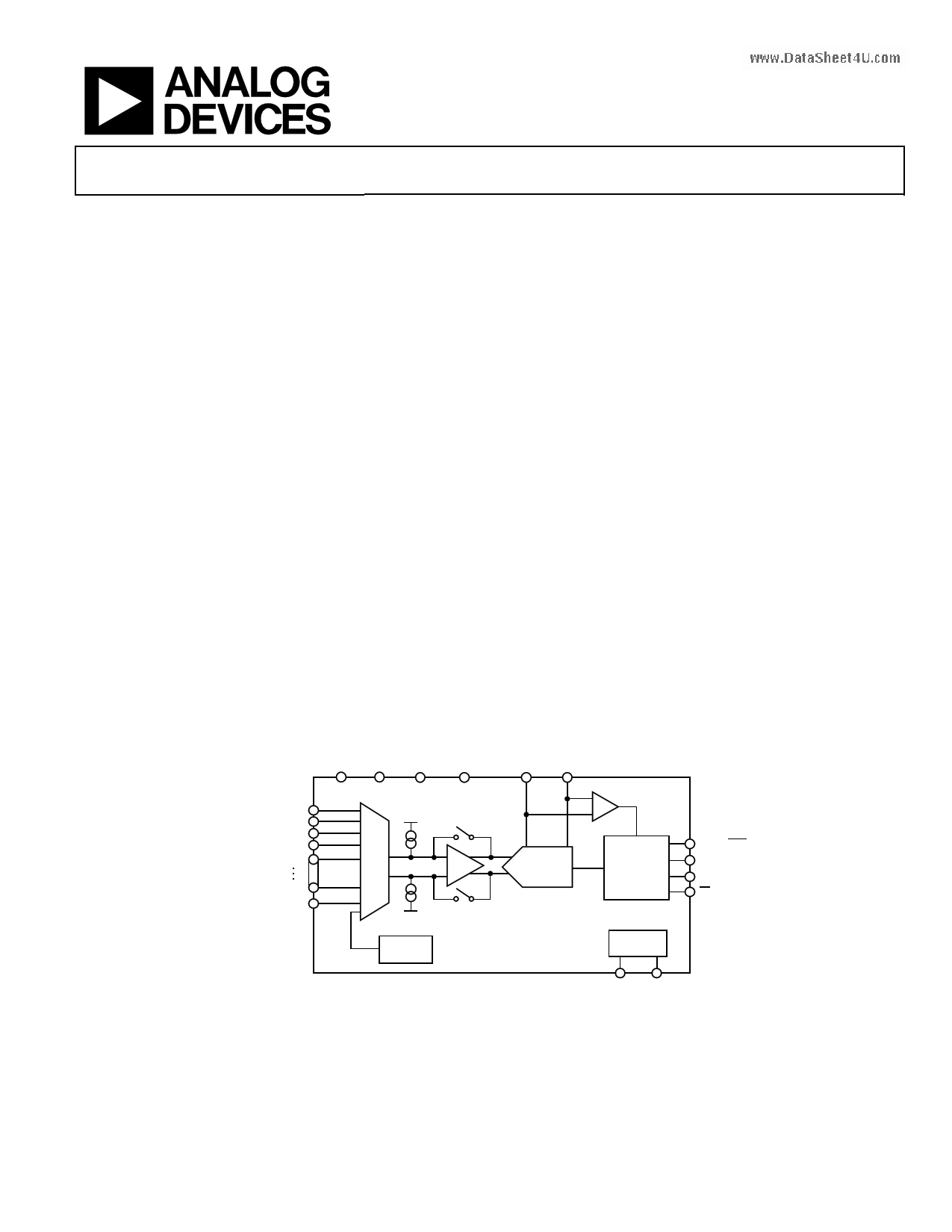
FUNCTIONAL BLOCK DIAGRAM
AVDD AGND DVDD DGND
REFIN1(+) REFIN1(–)
AIN1/P3
AIN2/P2
AIN3/P1/REFIN2(+)
AIN4/P0/REFIN2(–)
AIN5
AIN16
AINCOM
AVDD
AD7194
MUX
PGA
Σ-Δ
ADC
AGND
TEMP
SENSOR
REFERENCE
DETECT
SERIAL
INTERFACE
AND
CONTROL
LOGIC
DOUT/RDY
DIN
SCLK
CS
CLOCK
CIRCUITRY
Figure 1.
MCLK1 MCLK2
Rev. 0
Information furnished by Analog Devices is believed to be accurate and reliable. However, no
responsibility is assumed by Analog Devices for its use, nor for any infringements of patents or other
rights of third parties that may result from its use. Specifications subject to change without notice. No
license is granted by implication or otherwise under any patent or patent rights of Analog Devices.
Trademarksandregisteredtrademarksarethepropertyoftheirrespectiveowners.
One Technology Way, P.O. Box 9106, Norwood, MA 02062-9106, U.S.A.
Tel: 781.329.4700
www.analog.com
Fax: 781.461.3113
©2009 Analog Devices, Inc. All rights reserved.
1 page 
Parameter
REFERENCE INPUT
REFIN Voltage
Min
1
Absolute REFIN Voltage
Limits2
Average Reference Input
Current
Average Reference Input
Current Drift
AGND − 0.05
Normal Mode Rejection2
Common-Mode
Rejection
Reference Detect Levels
TEMPERATURE SENSOR
Accuracy
Sensitivity
BURNOUT CURRENTS
AIN Current
0.3
DIGITAL OUTPUTS (P0 to P3)
Output High Voltage, VOH
Output Low Voltage, VOL
AVDD − 0.6
4
Floating-State Leakage
Current2
Floating-State Output
Capacitance
INTERNAL/EXTERNAL CLOCK
Internal Clock
Frequency
Duty Cycle
External Clock/Crystal
www.DataShFereeqt4uUen.ccoym
Input Low Voltage, VINL
−100
4.72
2.4576
Input High Voltage, VINH
Input Current
LOGIC INPUTS
Input High Voltage, VINH2
Input Low Voltage, VINL2
Hysteresis2
Input Currents
LOGIC OUTPUT (DOUT/RDY)
Output High Voltage, VOH2
Output Low Voltage, VOL2
2.5
3.5
−10
2
0.1
−10
DVDD − 0.6
4
Floating-State Leakage
Current
Floating-State Output
Capacitance
Data Output Coding
−10
Typ Max
AVDD
4.5
±0.03
±1.3
Same as for
analog inputs
100
±2
2815
500
AVDD + 0.05
0.6
10
50:50
4.9152
0.4
0.4
+100
5.12
5.12
0.8
0.4
+10
0.8
0.25
+10
10
Offset binary
0.4
0.4
+10
Unit
V
V
μA/V
nA/V/°C
nA/V/°C
AD7194
Test Conditions/Comments1
REFIN = REFINx(+) − REFINx(−), the
differential input must be limited to
±(AVDD − 1.25 V)/gain when gain > 1
External clock
Internal clock
dB
V
°C
Codes/°C
nA
V
V
V
V
nA
pF
Applies after user calibration at 25°C
Bipolar mode
Analog inputs must be buffered and chop
disabled
AVDD = 3 V, ISOURCE = 100 μA
AVDD = 5 V, ISOURCE = 200 μA
AVDD = 3 V, ISINK = 100 μA
AVDD = 5 V, ISINK = 800 μA
MHz
%
MHz
V
V
V
V
μA
V
V
V
μA
V
V
V
V
μA
pF
DVDD = 5 V
DVDD = 3 V
DVDD = 3 V
DVDD = 5 V
DVDD = 3 V, ISOURCE = 100 μA
DVDD = 5 V, ISOURCE = 200 μA
DVDD = 3 V, ISINK = 100 μA
DVDD = 5 V, ISINK = 1.6 mA
Rev. 0 | Page 5 of 56
5 Page 
Pin No. Mnemonic
23 AVDD
24 DVDD
25 SYNC
26 NC
27 DOUT/RDY
28 DIN
29 MCLK1
30 MCLK2
31 SCLK
32 CS
www.DataSheet4U.com
AD7194
Description
Analog Supply Voltage, 3 V to 5.25 V. AVDD is independent of DVDD. Therefore, DVDD can be operated at 3 V
with AVDD at 5 V or vice versa.
Digital Supply Voltage, 2.7 V to 5.25 V. DVDD is independent of AVDD. Therefore, AVDD can be operated at 3 V
with DVDD at 5 V or vice versa.
Logic input that allows for synchronization of the digital filters and analog modulators when using a
number of AD7194 devices. While SYNC is low, the nodes of the digital filter, the filter control logic, and the
calibration control logic are reset, and the analog modulator is also held in its reset state. SYNC does not
affect the digital interface but does reset RDY to a high state if it is low. SYNC has a pull-up resistor
internally to DVDD.
This pin should be connected to GND for correct operation.
Serial Data Output/Data Ready Output. DOUT/RDY serves a dual purpose. It functions as a serial data
output pin to access the output shift register of the ADC. The output shift register can contain data from
any of the on-chip data or control registers. In addition, DOUT/RDY operates as a data ready pin, going low
to indicate the completion of a conversion. If the data is not read after the conversion, the pin goes high
before the next update occurs. The DOUT/RDY falling edge can be used as an interrupt to a processor,
indicating that valid data is available. With an external serial clock, the data can be read using the
DOUT/RDY pin. With CS low, the data-/control-word information is placed on the DOUT/RDY pin on the
SCLK falling edge and is valid on the SCLK rising edge.
Serial Data Input to the Input Shift Register on the ADC. Data in this shift register is transferred to the
control registers in the ADC, with the register selection bits of the communications register identifying the
appropriate register.
When the master clock for the device is provided externally by a crystal, the crystal is connected between
MCLK1 and MCLK2.
Master Clock Signal for the Device. The AD7194 has an internal 4.92 MHz clock. This internal clock can be
made available on the MCLK2 pin. The clock for the AD7194 can also be provided externally in the form of
a crystal or external clock. A crystal can be tied across the MCLK1 and MCLK2 pins. Alternatively, the MCLK2
pin can be driven with a CMOS-compatible clock and with the MCLK1 pin remaining unconnected.
Serial Clock Input. This serial clock input is for data transfers to and from the ADC. The SCLK has a Schmitt-
triggered input, making the interface suitable for opto-isolated applications. The serial clock can be
continuous with all data transmitted in a continuous train of pulses. Alternatively, it can be a nonconti-
nuous clock with the information transmitted to or from the ADC in smaller batches of data.
Chip Select Input. This is an active low logic input used to select the ADC. CS can be used to select the
ADC in systems with more than one device on the serial bus or as a frame synchronization signal in
communicating with the device. CS can be hardwired low, allowing the ADC to operate in 3-wire mode
with SCLK, DIN, and DOUT used to interface with the device.
Rev. 0 | Page 11 of 56
11 Page | ||
| Páginas | Total 30 Páginas | |
| PDF Descargar | [ Datasheet AD7194.PDF ] | |
Hoja de datos destacado
| Número de pieza | Descripción | Fabricantes |
| AD7190 | 4.8 kHz Ultra-Low Noise 24-Bit Sigma-Delta ADC | Analog Devices |
| AD7191 | Sigma-Delta ADC | Analog Devices |
| AD7192 | 4.8 KHz Ultra-Low Noise 24-Bit Sigma-Delta ADC | Analog Devices |
| AD7193 | 24-Bit Sigma-Delta ADC | Analog Devices |
| Número de pieza | Descripción | Fabricantes |
| SLA6805M | High Voltage 3 phase Motor Driver IC. |
Sanken |
| SDC1742 | 12- and 14-Bit Hybrid Synchro / Resolver-to-Digital Converters. |
Analog Devices |
|
DataSheet.es es una pagina web que funciona como un repositorio de manuales o hoja de datos de muchos de los productos más populares, |
| DataSheet.es | 2020 | Privacy Policy | Contacto | Buscar |